
Videos
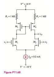
Consider the diff-amp in Figure P11.68. The PMOS parameters are:
(a)
The open circuit differential mode voltage gain.
Answer to Problem 11.68P
The value of the differential mode voltage gain is
Explanation of Solution
Given:
The given circuit is shown in Figure 1
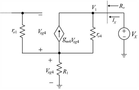
Figure 1
Calculation:
From above, the expression for the source to gate voltage is given by,
Apply KCL at node
Substitute
The expression for the transconductance of the second transistor is evaluated as,
Substitute
The internal output resistance of the second transistor is given by,
Substitute
The expression for the transconductance of the fourth transistor is evaluated as,
Substitute
The internal output resistance of the fourth transistor is given by,
Substitute
The expression to determine the value of the resistance
Substitute
The expression to determine the value of the open circuit differential mode voltage gain is given by,
Substitute
Conclusion:
Therefore, the value of the open circuit differential mode voltage gain is
(b)
To compare: The value of the open circuit differential mode voltage gain for the given changes with the value obtained in part (a).
Answer to Problem 11.68P
The value of the differential voltage gain is
Explanation of Solution
Given:
The given circuit is shown in Figure 1
Figure 1
The value of resistance
Calculation:
When
The expression for the open circuit differential mode voltage gain is given by,
Substitute
When the resistance
Conclusion:
Therefore, the value of the differential voltage gain is
(c)
The value of the output resistance of the differential amplifier for part (a) and (b).
Answer to Problem 11.68P
The differential output resistance of the amplifier for part (a) is
Explanation of Solution
The given circuit is shown in Figure 1

Figure 1
Calculation:
The output resistance for the differential amplifier for the open circuit differential voltage gain is calculated as,
Substitute
The output resistance for the differential amplifier when
Substitute
Conclusion:
Therefore, the differential output resistance of the amplifier is
Want to see more full solutions like this?
Chapter 11 Solutions
Microelectronics: Circuit Analysis and Design


- Design a self-biased JFET circuit (Fig. 6) assuming VGS(0) = -1.3 and ipss= 20 mA. We require a VGS = -0.7. Assume a supply voltage of 15 volts. Draw the load line for this circuit using Fig. 4b once you have selected the appropriate values for the components. Does the load line intersect the VGS = -0.7 volt line at the computed in point? RD. RG Rs 12 20nA GS = -1.3 VGS 10nA Fig. 6. Circuit for Examples 2 &3. 50 100 150 200 □ ID(J1) UDS Fig. 4b. The IV characteristics of an n-channel JFET (J113). The plots are for VGs increments of 0.05 volts. VGS(0) -1.3. The yellow and blue load lines are for examples 2 &3, respectively.arrow_forwardFind the operating point and the load line of a voltage-divider JFET biasing circuit using the following parameters: VGS(0) = -1.3 and Vcc = 15 volts. Assume ipss = 20 mA, RG₁ = RG2 = 10 kn, RD = 300, and Rs = 1 kn. Use Fig. 4b for the IV characteristic of the JFET. 20nA GS=-1.3 GS 10nA- 50 100 150 200 ID(J1) UDS Fig. 4b. The IV characteristics of an n-channel JFET (J113). The plots are for VGs increments of 0.05 volts. VGS(0) -1.3. The yellow and blue load lines are for examples 2 &3, respectively.arrow_forwardDesign the JFET circuit for the largest in swing. Use the self-bias circuit shown in Fig. 6. Assume that VGS (0) = -1.3 and Vcc = 15 volts. Furthermore, assume that ipss = 20 mA. Using Fig. 4b, draw the load line and identify the Q point. Explain why this will allow the largest swing. Use ip = ipss (1- VGS VGS(0) to show what happens to i, and vps when you have a swing of 0.2 volts in vcs form its operating point (that is, change vas by ±0.2 volts and compute the corresponding iD and VDs). RD RG Rs 0 20nA GS=-1.3 VGS 12 10nA -0- Fig. 6. Circuit for Examples 2 &3. BA-C 50 100 150 200 □ ID(J1) UDS Fig. 4b. The IV characteristics of an n-channel JFET (J113). The plots are for VGs increments of 0.05 volts. VGS(0) -1.3. The yellow and blue load lines are for examples 2 &3, respectively.arrow_forward
- please do the correct VI chrastaristics curve on excel. I am not sure if mine is correctarrow_forwardplease do the correct VI chrastaristics curve on excel. I am not sure if mine is correct. Note the two curves in the picture are for both but its two tries and i dont know which is correct, and probebly both are wrong SCR (Forward Bias Condition) NO VAA VG= 0V, IG=0 mA VG= 5V, IG=4.07mA VG= 10V, IG=9.05mA VAK (V) IAK(mA) VAK (V) IAK(mA) VAK (V) IAK(mA) 1 0 0 0 0 0 0 0 2 5 0.576 4.42 mA 0.576 4.42 mA 0.576 4.43 3 10 7.99 2 0.598 9.4 0.598 9.4 4 15 14.99 0.003 0.612 14.4 0.612 14.4 5 20 19.994 0.004 0.622 19.4 0.622 19.4 6 25 0.63 24.4 0.63 24.4 0.63 24.4 4 30 0.637 29.4 0.637 29.4 0.637 29.4 8 40 0.65 39.4 0.65 39.4 0.65 39.4 9 50 0.66 49.3 0.66 49.3 0.66 49.3 10 60 0.67 59.3 0.67 59.3 0.67 59.3 11 70 0.679 69.3 0.679 69.3 SCR (Reversed Bias…arrow_forwardSee both images attachedarrow_forward
- 5 Find the value of voltage Vy using nodal analysis (write and then solve the set of equations to get voltage Vx from your variables.) 43 LX + Vx да ww 1 23 дъх 83 38 wwarrow_forwardhelp on this question about block diagram reduction?arrow_forward4) Find the valve of current if using nodal analys.3. (write and then solve the set of equations toget current Ex from your voltage variables.) M 3 ча + GA हुप 8Aarrow_forward
 Introductory Circuit Analysis (13th Edition)Electrical EngineeringISBN:9780133923605Author:Robert L. BoylestadPublisher:PEARSON
 Delmar's Standard Textbook Of ElectricityElectrical EngineeringISBN:9781337900348Author:Stephen L. HermanPublisher:Cengage Learning
 Programmable Logic ControllersElectrical EngineeringISBN:9780073373843Author:Frank D. PetruzellaPublisher:McGraw-Hill Education
 Fundamentals of Electric CircuitsElectrical EngineeringISBN:9780078028229Author:Charles K Alexander, Matthew SadikuPublisher:McGraw-Hill Education
 Electric Circuits. (11th Edition)Electrical EngineeringISBN:9780134746968Author:James W. Nilsson, Susan RiedelPublisher:PEARSON
 Engineering ElectromagneticsElectrical EngineeringISBN:9780078028151Author:Hayt, William H. (william Hart), Jr, BUCK, John A.Publisher:Mcgraw-hill Education,