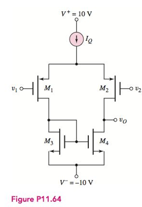
The differential amplifier in Figure P11.64 has a pair of PMOS transistors as input devices and a pair of NMOS transistors connected as an active load. The circuit is biased with I Q = 0.2 mA , and the transistor parameters are: K n = K p = 0.1 mA / V 2 , λ n = 0.01 V − 1 , λ p = 0.015 V − 1 V T N = 1 V , and V T P = − 1 V . (a) Determine the quiescent drain-to source voltage in each transistor. (b) Find the open-circuit differential mode voltage gain. (c) What is the output resistance?
The differential amplifier in Figure P11.64 has a pair of PMOS transistors as input devices and a pair of NMOS transistors connected as an active load. The circuit is biased with I Q = 0.2 mA , and the transistor parameters are: K n = K p = 0.1 mA / V 2 , λ n = 0.01 V − 1 , λ p = 0.015 V − 1 V T N = 1 V , and V T P = − 1 V . (a) Determine the quiescent drain-to source voltage in each transistor. (b) Find the open-circuit differential mode voltage gain. (c) What is the output resistance?
Solution Summary: The diagram shows the value of the quiescent drain to source voltage in each transistor.
The differential amplifier in Figure P11.64 has a pair of PMOS transistors as input devices and a pair of NMOS transistors connected as an active load. The circuit is biased with
I
Q
=
0.2
mA
,
and the transistor parameters are:
K
n
=
K
p
=
0.1
mA
/
V
2
,
λ
n
=
0.01
V
−
1
,
λ
p
=
0.015
V
−
1
V
T
N
=
1
V
,
and
V
T
P
=
−
1
V
.
(a) Determine the quiescent drain-to source voltage in each transistor. (b) Find the open-circuit differential mode voltage gain. (c) What is the output resistance?
Don't use guidelines okk just solve all accurate only 100% sure experts solve it correct complete solutions okkk
3. Consider the circuit, in which R₁ = 10 KQ2, R2 =
5 KQ, R3 = 1 KQ, and RE = 8 KQ. The supply
voltages are +Vcc = 10 V and -VEE = -5 V. Other
parameters are ẞF = 100, VBE(On) = 0.7 V, and
VCE(Sat) 0.2 V. Rc value will be specified later.
(a) (3 points) Draw the dc equivalent circuit of the
circuit.
VI
+Vcc
Rc
R2
RI
R₁
RE
-VEE
υο
R3
(b) Find the Thevenin equivalent voltage source VEQ and input resistance REQ of the DC
equivalent circuit. Show your work.
+Vcc
Rc
UC
VEQ
www
REQ
VE
VEQ =
REQ =
ΚΩ
RE
VEE
5. Consider the ac equivalent circuit of an
amplifier, where RE = 1 KS2, gm = 0.05 S, and
Υπ= 2Κ Ω.
(a) Redraw the ac equivalent circuit using the
hybrid-pi small signal model for BJTS.
Include ro in the model.
R₁
ww
Vi
RB
ww
+
RL
Vo
RE
(b) Find the terminal resistance RIB using the circuit obtained in (a). Ignore ro. Show your
work. (Don't use formula for RiB.)
Need a deep-dive on the concept behind this application? Look no further. Learn more about this topic, electrical-engineering and related others by exploring similar questions and additional content below.


 Introductory Circuit Analysis (13th Edition)Electrical EngineeringISBN:9780133923605Author:Robert L. BoylestadPublisher:PEARSON
 Delmar's Standard Textbook Of ElectricityElectrical EngineeringISBN:9781337900348Author:Stephen L. HermanPublisher:Cengage Learning
 Programmable Logic ControllersElectrical EngineeringISBN:9780073373843Author:Frank D. PetruzellaPublisher:McGraw-Hill Education
 Fundamentals of Electric CircuitsElectrical EngineeringISBN:9780078028229Author:Charles K Alexander, Matthew SadikuPublisher:McGraw-Hill Education
 Electric Circuits. (11th Edition)Electrical EngineeringISBN:9780134746968Author:James W. Nilsson, Susan RiedelPublisher:PEARSON
 Engineering ElectromagneticsElectrical EngineeringISBN:9780078028151Author:Hayt, William H. (william Hart), Jr, BUCK, John A.Publisher:Mcgraw-hill Education,