
The design parameters for the BJT differential amplifier with the active load and the mode voltage gain.
Answer to Problem D11.71P
The value of the differential voltage gain is
Explanation of Solution
Given:
The given circuit is shown in Figure 1
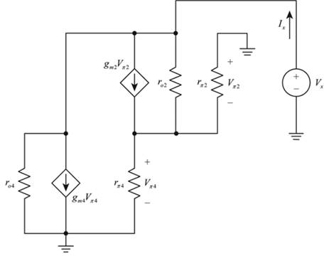
Figure 1
Calculation:
The expression for the input current is given by,
The expression to determine the value of the transconductance is given by,
The expression for the relation for the voltage for hybrid pie parameter.
Substitute
The value of the collector current
The value of the collector current
The expression to determine the expression for the diffusion resistance is given by,
Substitute
The value of the transconductance is calculated as,
Substitute
The expression to determine the value of the resistance
Substitute
The expression to determine the expression for the diffusion resistance is given by,
Substitute
The value of the transconductance is calculated as,
Substitute
The expression to determine the value of the resistance
Substitute
Substitute
The expression for the input current
Substitute
Substitute
The expression to determine the output resistance is given by,
Substitute
The value of the quiescent current is given by,
The small signal output resistance is calculated as,
The value of the output resistance is calculated as,
The required small signal circuit is shown in Figure 2
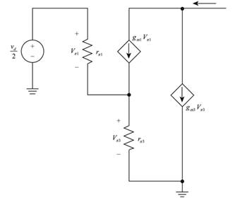
Figure 2
The expression for the transconductance is given by,
The expression for the differential voltage gain is given by,
The expression for the change in current is given by,
Consider the value of
Substitute the values in the above equation.
Substitute
Substitute
Substitute
Substitute
The value of gain is given by,
The expression for the input resistor is given by,
The value of expression for the differential input resistor is calculated as,
Conclusion:
Therefore, the value of the differential voltage gain is
Want to see more full solutions like this?
Chapter 11 Solutions
Microelectronics: Circuit Analysis and Design

- Circuits help please solve and explain. Question in images providedarrow_forward+ V 6.2 A 1.2 A S R 4 Ω Find the source voltage Vs 0.8 Aarrow_forwardDetermine i(t) for t≥ 0 given that the circuit below had been in steady state for a long time prior to t = 0. Also, I₁ = 1 5 A, R₁ =22, R2 =10 Q2, R3 = 32, R4 =7 2, and L=0.15 H. Also fill the table. m L ww R2 t = 0 R₁ 29 R3 R4 Time 0 iL(t) 0 8arrow_forward
- Find the Thévenin equivalent circuit for the portions of the networks in Figure external to the elements between points a and b. a R₁ 2002 I = 0.1 A 0° Xc : 32 Ω R2 = 6802 20 Ω фъarrow_forwardFind the Norton equivalent circuit for the network external to the elements between a and b for the networks in Figure. E1 = 120 V Z 0° R ww 10 Ω Xc XL · 000 802 802 ① I = 0.5 AZ 60° ZL barrow_forwardUsing superposition, determine the current through inductance XL for each network in Figure I = 0.3 A 60° XL 000 802 XC 502 Ω E 10 V0° =arrow_forward
- Find the Thévenin equivalent circuit for the portions of the networks in Figure external to the elements between points a and b. E = 20 VZ0° + R ww 2 ΚΩ Хо XL 000 6ΚΩ 3 ΚΩ b RLarrow_forwardWhat percentage of the full-load current of a thermally protected continuous-duty motor of more than one Hp can the trip current be, if the full-load current is 15 amperes? Ο 122 Ο 140 156 O 170arrow_forwardQ3arrow_forward
 EBK ELECTRICAL WIRING RESIDENTIALElectrical EngineeringISBN:9781337516549Author:SimmonsPublisher:CENGAGE LEARNING - CONSIGNMENT