
The design parameters for the BJT differential amplifier with the active load and the mode voltage gain.
Answer to Problem D11.71P
The value of the differential voltage gain is
Explanation of Solution
Given:
The given circuit is shown in Figure 1
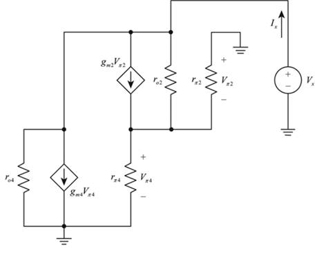
Figure 1
Calculation:
The expression for the input current is given by,
The expression to determine the value of the transconductance is given by,
The expression for the relation for the voltage for hybrid pie parameter.
Substitute
The value of the collector current
The value of the collector current
The expression to determine the expression for the diffusion resistance is given by,
Substitute
The value of the transconductance is calculated as,
Substitute
The expression to determine the value of the resistance
Substitute
The expression to determine the expression for the diffusion resistance is given by,
Substitute
The value of the transconductance is calculated as,
Substitute
The expression to determine the value of the resistance
Substitute
Substitute
The expression for the input current
Substitute
Substitute
The expression to determine the output resistance is given by,
Substitute
The value of the quiescent current is given by,
The small signal output resistance is calculated as,
The value of the output resistance is calculated as,
The required small signal circuit is shown in Figure 2
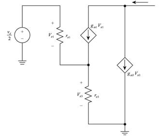
Figure 2
The expression for the transconductance is given by,
The expression for the differential voltage gain is given by,
The expression for the change in current is given by,
Consider the value of
Substitute the values in the above equation.
Substitute
Substitute
Substitute
Substitute
The value of gain is given by,
The expression for the input resistor is given by,
The value of expression for the differential input resistor is calculated as,
Conclusion:
Therefore, the value of the differential voltage gain is
Want to see more full solutions like this?
Chapter 11 Solutions
MICROELECT. CIRCUIT ANALYSIS&DESIGN (LL)

- Use the ramp generator circuit in Fig. B2a to generate the waveform shown in Fig. B2b. Write four equations relating resistors R1, R2, R3, capacitor C and voltages Vs, VR and VA.to the waveform parameters T₁, T, Vcm and Vm- If R = R2 = R3, R₁ = 2R, C = 1 nF, Vcm = 2 V and Vm = 1 V, T₁ = 2 μs and T = 10 μs solve for the values of R, Vs, VR and VA using your equations from part a(i). VR C +VA R3 V₂ Vo мат R1 VsO+ V₁ R₂ Figure B2a Vout Vcm+Vm Vcm Vcm-Vm 0 T₁ T 2T time Figure B2barrow_forwardThe circuit in Figure B1a is a common analogue circuit block. Explain why you would need such a circuit. Draw another circuit in which you use the current flowing in this loop to bias a common source amplifier. This circuit is not ideal for standard CMOS technologies due to threshold shift. Why? Draw an improved version of this circuit to make it better. VDD (W)P MA M3. (), REF (쁜)~ M₁ M2 lout 시~ Rsarrow_forward23bcarrow_forward
- Draw the small-signal equivalent circuit of a single transistor amplifier given in figure B1b. Assume the current source to be ideal. Determine the Open-loop transfer function, pole frequency and gain-bandwidth product all in terms of transistor parameters 9m, To and CL. If the load capacitance is 1pF and the necessary unity gain frequency is 600MHz, find the gm for this transistor. V₁ V₁ CLarrow_forward23baarrow_forward23caarrow_forward
 EBK ELECTRICAL WIRING RESIDENTIALElectrical EngineeringISBN:9781337516549Author:SimmonsPublisher:CENGAGE LEARNING - CONSIGNMENT