
Concept explainers
Videos
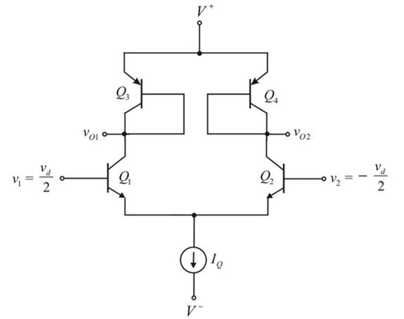
Consider the diff-amp shown in Figure P 11.62 . The circuit parameters are
(a)
To sketch: The small signal equivalent circuit for the differential amplifier.
Answer to Problem 11.62P
The small signal circuit is shown in Figure 2.
Explanation of Solution
Given:
The given circuit is shown below.

Calculation:
The small signal equivalent circuit for the above circuit is shown in Figure 1.
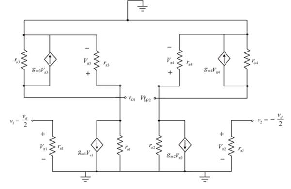
Figure 1
Because of symmetry the value of the currents
The value of the currents
The value of the currents
The value of the currents
For differential up circuit emitter current
Modify the circuit, the required diagram is shown in Figure 2
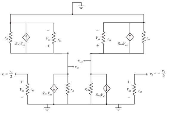
Figure 2
Conclusion:
Therefore, the small signal circuit is shown in Figure 3
(b)
The value of one sided differential voltage gain.
Answer to Problem 11.62P
The value of the differential mode voltage gain is
Explanation of Solution
Given:
The given circuit is shown below.
 Calculation:
Consider the left portion of the circuit as,
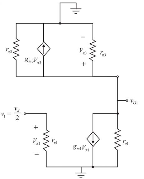
Figure 3
Modify the circuit as shown in Figure 4
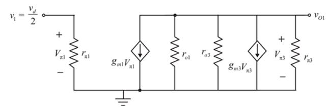
Figure 4
The expression for the output voltage of the above circuit is given by,
The emitter current of the transistor is calculated as,
The expression for the collector current of the transistor
Substitute
Apply KCL at the output node
Substitute
The transconductance of transistor
The transconductance of transistor
The small signal output resistance of
The small signal output resistance of
The small signal resistance
The value of the voltage
Conclusion:
Therefore, the value of the differential mode voltage gain is
(c)
The differential voltage gain of both the sides.
Answer to Problem 11.62P
The value of differential voltage gain is
Explanation of Solution
Given:
The given circuit is shown below.

Calculation:
The expression for the output voltage of the above circuit is given by,
The value of the voltage
Conclusion:
Therefore, the value of differential voltage gain is
(d)
The value of the differential voltage gain of both the sides.
Answer to Problem 11.62P
The value of differential voltage gain is
Explanation of Solution
Given:
The given circuit is shown below.

Calculation:
The expression to determine the value of the two sided differential voltage gain is given by,
Conclusion:
Therefore, the value of differential voltage gain is
Want to see more full solutions like this?
Chapter 11 Solutions
MICROELECT. CIRCUIT ANALYSIS&DESIGN (LL)


- Q3. a) The frequency response method enables the study of the steady-state response of a system G(s). What type of inputs are used for frequency response? If the system is linear and stable, how does the output differ from the input? Compare the main characteristics of two types frequency response plots. b) Consider the control system shown in Figure Q3. Controller E(s) R(s) Desired output C(s) Plant G(s) Y(s) Actual output 3(s + 3) C(s) = k G(s) = = s(s - 1)(s + 10) Figure Q3. Closed-loop system. (i) Considering definitions in the study of bounded-input bounded-output stability, is G(s) stable? Classify the poles and zeros of G(s). (ii) G(s) defined in Figure Q3 is a system completely characterised by its transfer function. Explain why this is the case. (iii) Obtain the closed-loop transfer function P(s) = Y(s)/R(s) of the system. (iv) Based on your result for the previous question [Question 3b)-(iii)], use the Routh-Hurwitz stability criterion to determine suitable values of gain K…arrow_forwardPlease, I want the solution in two ways: Method 1 (without the Smith chart): Method 2 (using the Smith chart): A short circuit stub of length 0.04λ is used to match a 50 Ω lossless line to a load ZL = RL + j30 Ω. Use Smith chart to find:(a) The distance between the stub and the load.(b) The value of RL .arrow_forwardTHE FIRST PAGE OF THIS QUESTION SECTION BELOW IS THE FIRST IMAGE UPLOADED, WHICH SHOWS A digital synchronous sequential circuit and then comes the questions below:1B) Suppose the flip-flops are 74F74 devices and the AND gates are 74F08 devices. Let maxtpd,D=9ns, maxtsu,D=3ns, and maxtpd,AND=6ns. What is the maximum clock frequency at which the circuit can operate reliably? 2) Compare serial transmission and parallel transmission and discuss their advantages and disadvantages. 3) Explain briefly how the slave can protect itself from being overwhelmed by the master in I2 4) A hypothetical logic family has the following specifications. VOH=4.6V VIH=4.0V VOL=0.5V VIL=1.0V IOH=-1mA IIH=50μA IOL=8mA IIL=-0.6mA (4a) What are the noise margins? (4b) What is the fan-out capability?…arrow_forward
- THE FIRST PAGE OF THIS QUESTION SECTION BELOW IS THE FIRST IMAGE UPLOADED, WHICH SHOWS A digital synchronous sequential circuit and then comes the questions below:1B) Suppose the flip-flops are 74F74 devices and the AND gates are 74F08 devices. Let maxtpd,D=9ns, maxtsu,D=3ns, and maxtpd,AND=6ns. What is the maximum clock frequency at which the circuit can operate reliably? 2) Compare serial transmission and parallel transmission and discuss their advantages and disadvantages. 3) Explain briefly how the slave can protect itself from being overwhelmed by the master in I2 4) A hypothetical logic family has the following specifications. VOH=4.6V VIH=4.0V VOL=0.5V VIL=1.0V IOH=-1mA IIH=50μA IOL=8mA IIL=-0.6mA (4a) What are the noise margins? (4b) What is the fan-out capability?…arrow_forwardI need help on this question a) Find y(t) =yh(t) +yp(t) in time domainIs the system over-damped, under-damped, or critical?arrow_forwardGiven f(t)=a sin(ßt) a = 10 & ß = 23 Find the Laplace Transform using the definition F(s) = ∫f(t)e-stdtarrow_forward
- = Calculate Avf, Zif, and Zof for the amplifier circuit,Assume he = 50, hie 1.1k2, and identical transistors? 150kQ Vs 5002 HH +25v 10k +6 · 47ΚΩ 47k2 4.7k0} 33 ΚΩ 4.7ΚΩ 10k w 4.7kQ HH Voarrow_forwardFor the four-pole filter in Fig. (2), determine the capacitance values required to produce a critical frequency of 2680 Hz if all the resistors in the RC low-pass circuits are 1.8 K. Also select values for the feedback resistors to get a Butterworth response. Note: For a Butterworth response, the damping factor must be 1.848 for the first stage and 0.765 for the second stage. (2) Re Res ww " = 11arrow_forwardFor the circuit shown in Fig. 2.20, the transistors are identica' and have the following parameters: hje=50, hie = 1.1K, hr =0, and hoe = 0. Calculate Auf, Rif and Rof. Ans: 45.4; 112 KN; 129N. HH 150k 47k R 25 V 10k 47k 4.7k 5μF 33k 4.7k 50µF 50µF 4.7k 4.7k R₁ Roj R1000arrow_forward
- A triangular wave is applied to the input of Fig. (3). Determine what the output should be and sketch its waveform in relation to the input. 10μs. 0 5μs 15 μs 0.001 μF R₁ w 2.2karrow_forwardA three-phase, 480-V, 60-Hz, 6-pole, Y-connected induction motor has its speed controlled by slip power. The circuit parameters are given: Rs=0.06 ohms, Rr=0.05 ohms, Xs=0.2 ohms, Xr=0.3 ohms and Xm=6 ohms. The turn ratio of the rotor to stator winding is n=0.8. The no-load losses of the motor are equal to 150 W. The rotor and stator cupper losses are equal to 249.21 W. The slip power losses are estimated to 8000W. The load torque is 173.61 N.m. at 700 rpm. The efficiency is equal to: Select one: a. 71.5% b. None of these c. 81.5% d. 91.5% Question 2 Consider a 3-phase, 460-V, 100-hp, 0.88 power factor lagging, 4-pole, 1728 RPM, 60 Hz, Y-connected induction motor. The operating slip is equal to: Select one: a. 0.05 b. 0.01 c. 0.04 d. None of these Question 3 A 3 phase, 10 kW, 1750 rpm, Y- connected 460 V, 60 Hz, 4 poles, Y-connected induction motor has the following parameters: Rs = 0.5 Ohms, Rr = 0.3 Ohms, Xs = 0.9 Ohms, Xr = 0.9 Ohms, Xm = 25 Ohms. The no load…arrow_forwardelectric plants do for hand writingarrow_forward
 EBK ELECTRICAL WIRING RESIDENTIALElectrical EngineeringISBN:9781337516549Author:SimmonsPublisher:CENGAGE LEARNING - CONSIGNMENT