MICROELECT. CIRCUIT ANALYSIS&DESIGN (LL)
4th Edition
ISBN: 9781266368622
Author: NEAMEN
Publisher: MCG
bartleby

Videos

Question
Book Icon
Chapter 11, Problem 11.84P

a.

To determine

The small-signal voltage gain Av=vo/vi and the output resistance Ro for the given circuit.

a.

Expert Solution
Check Mark

Answer to Problem 11.84P

  Av=30053Ro=192.2MΩ

Explanation of Solution

Given:

The given circuit is,
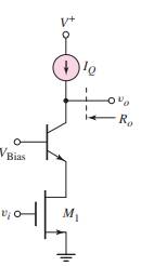
  MICROELECT. CIRCUIT ANALYSIS&DESIGN (LL), Chapter 11, Problem 11.84P , additional homework tip  1

  IQ=25μA,β=100VA=50V,VTN=0.8V,Kn=0.25mA/V2,λ=0.02V1

The two amplifying transistors M1andQ1 are biased in the saturation region and forward-active region.

Calculation:

Consider the given figure,

  Ic=IQ=25μA,

Now find trans-conductance,

  gm2=IcVT=25×10626×103gm2=0.9615mA/VNowfindrπ,rπ=βVTIc=(100)26×10325×106rπ=104kΩnowgm1gm1=2kpIQgm1=20.25×103(25×106)gm1=0.158mA/V

Now calculate r01,r02 ,

  r01=1λIQ=1(0.02)25μAr01=2MΩr02=VAIQ=5025μAr02=2MΩ

Now consider small-signal equivalent circuit,
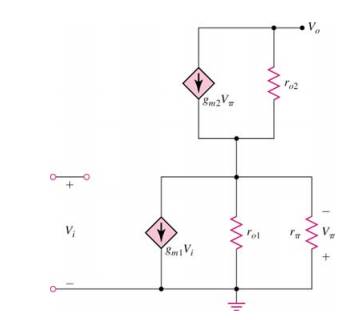
  MICROELECT. CIRCUIT ANALYSIS&DESIGN (LL), Chapter 11, Problem 11.84P , additional homework tip  2

Apply nodal method at node Vπ ,

  VπrπVπr01+gm1Vi=0Vπ=(rπr01gm1rπ+r01)ViPutthevalues,Vπ=((104×103)(2×10⁶)(0.158×10³)(104×103)+(2×10⁶))ViVπ=15.62Vi

Now apply nodal method at node Vo ,

  Vo(Vπ)r02gm2Vπ=0Vo(1r02)+Vπ(1r02+gm2)=0Putthevalues,Vo(12×106)+15.62Vi(12×106+0.9615×10³)=0Vo=30053ViAv=30053

Now consider,

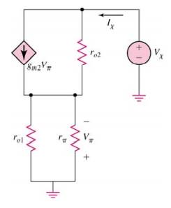
  MICROELECT. CIRCUIT ANALYSIS&DESIGN (LL), Chapter 11, Problem 11.84P , additional homework tip  3

Find Vπ ,

  Vπ=Ix(r01||rπ)Vπ=Ix(r01rπr01+rπ)Vπ=Ix((2×10⁶)(104×103)(2×10⁶)+(104×103))Vπ=9868×103Ix

Apply nodal analysis at node Vx ,

  Ix=gm2Vπ+Vx(Vπ)r02Ix=gm2Vπ+Vx+Vπr02Ix=(0.9615×10³)(98.86×10³)Ix+Vx(98.86×103)Ix(2×106)VxIx=Ro=96.1(2×10⁶)Ro=192.2MΩ

Hence,

  Av=30053Ro=192.2MΩ

b.

To determine

The small-signal voltage gain Av=vo/vi and the output resistance Ro for the given circuit.

b.

Expert Solution
Check Mark

Answer to Problem 11.84P

  Av=5.80×10⁷Ro=192.2MΩ

Explanation of Solution

Given:

The given circuit is,
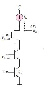
  MICROELECT. CIRCUIT ANALYSIS&DESIGN (LL), Chapter 11, Problem 11.84P , additional homework tip  4

  IQ=25μA,β=100VA=50V,VTN=0.8V,Kn=0.25mA/V2,λ=0.02V1

The two amplifying transistors M1andQ1 are biased in the saturation region and forward-active region.

Calculation:

Consider the given figure,

  Ic=IQ=25μA,

Now find trans-conductance,

  gm1=IcVT=25×10626×103gm1=0.9615mA/Vgm1=gm2=0.9615mA/VNowfindrπ,forQ1rπ1=βVTIc=(100)26×10325×106rπ1=104kΩrπ1=rπ2=104kΩ

Now,

  gm3=2kpIQgm3=20.25×10³(25×106)gm3=0.158mA/V

  r03=1λIQr03=10.02(25×106)r03=2MΩr01=VAIQr01=50(25×106)r01=2MΩr01=r02=2MΩ

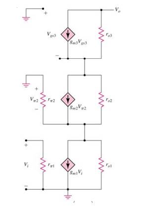
Now consider circuit,

  MICROELECT. CIRCUIT ANALYSIS&DESIGN (LL), Chapter 11, Problem 11.84P , additional homework tip  5

Apply nodal at top part of the circuit,

  Vo(Vgs)r03gm3Vgs=0Vo(1r03)=+Vgs(1r03+gm3)Vgs=(11+gm3r03)Voputthevalues,Vgs=(11+(0.158×10³)2×10⁶)VoVgs=Vo/317

Apply nodal at middle part of the circuit,

  Vgs(Vπ2)r02gm2Vπ2=0Vgs(1r02)+Vπ2(1r02+gm2)=0Vπ2=(11+gm2r02)Vgsputthevalues,Vπ2=(11+0.9615×10³(2×10⁶))(Vo317)Vπ2=Vo/725348

  Vo=117.28×10⁷ViVπ=1923ViVgs=3699852Vi

  Av=Vo/ViAv=5.80×107

Find Vπ ,

  Vπ=Ix(r01||rπ)Vπ=Ix(r01rπr01+rπ)Vπ=Ix((2×10⁶)(104×103)(2×10⁶)+(104×103))Vπ=9868×103Ix

Apply nodal analysis at node Vx ,

  Ix=gm2Vπ+Vx(Vπ)r02Ix=gm2Vπ+Vx+Vπr02Ix=(0.9615×10³)(98.86×10³)Ix+Vx(98.86×103)Ix(2×106)VxIx=Ro=96.1(2×10⁶)Ro=192.2MΩ

Hence,

  Av=5.80×10⁷Ro=192.2MΩ

Want to see more full solutions like this?

Subscribe now to access step-by-step solutions to millions of textbook problems written by subject matter experts!
Students have asked these similar questions
No chatgpt pls will upvote
circuit find value of VAB using Super Position Theorem
dc circuit vth rth rl thevenin and then maximum transer and value of rl

Chapter 11 Solutions

MICROELECT. CIRCUIT ANALYSIS&DESIGN (LL)

Ch. 11 - Prob. 11.7EPCh. 11 - Prob. 11.4TYUCh. 11 - Prob. 11.5TYUCh. 11 - The parameters of the diff-amp shown in Figure...Ch. 11 - For the differential amplifier in Figure 11.20,...Ch. 11 - The parameters of the circuit shown in Figure...Ch. 11 - The circuit parameters of the diff-amp shown in...Ch. 11 - Consider the differential amplifier in Figure...Ch. 11 - The diff-amp in Figure 11.19 is biased at IQ=100A....Ch. 11 - Prob. 11.10TYUCh. 11 - The diff-amp circuit in Figure 11.30 is biased at...Ch. 11 - Prob. 11.11EPCh. 11 - Prob. 11.12EPCh. 11 - Prob. 11.11TYUCh. 11 - Prob. 11.12TYUCh. 11 - Redesign the circuit in Figure 11.30 using a...Ch. 11 - Prob. 11.14TYUCh. 11 - Prob. 11.15TYUCh. 11 - Prob. 11.16TYUCh. 11 - Prob. 11.17TYUCh. 11 - Consider the Darlington pair Q6 and Q7 in Figure...Ch. 11 - Prob. 11.14EPCh. 11 - Consider the Darlington pair and emitter-follower...Ch. 11 - Prob. 11.19TYUCh. 11 - Prob. 11.15EPCh. 11 - Consider the simple bipolar op-amp circuit in...Ch. 11 - Prob. 11.17EPCh. 11 - Define differential-mode and common-mode input...Ch. 11 - Prob. 2RQCh. 11 - From the dc transfer characteristics,...Ch. 11 - What is meant by matched transistors and why are...Ch. 11 - Prob. 5RQCh. 11 - Explain how a common-mode output signal is...Ch. 11 - Define the common-mode rejection ratio, CMRR. What...Ch. 11 - What design criteria will yield a large value of...Ch. 11 - Prob. 9RQCh. 11 - Define differential-mode and common-mode input...Ch. 11 - Sketch the de transfer characteristics of a MOSFET...Ch. 11 - Sketch and describe the advantages of a MOSFET...Ch. 11 - Prob. 13RQCh. 11 - Prob. 14RQCh. 11 - Describe the loading effects of connecting a...Ch. 11 - Prob. 16RQCh. 11 - Prob. 17RQCh. 11 - Prob. 18RQCh. 11 - (a) A differential-amplifier has a...Ch. 11 - Prob. 11.2PCh. 11 - Consider the differential amplifier shown in...Ch. 11 - Prob. 11.4PCh. 11 - Prob. D11.5PCh. 11 - The diff-amp in Figure 11.3 of the text has...Ch. 11 - The diff-amp configuration shown in Figure P11.7...Ch. 11 - Consider the circuit in Figure P11.8, with...Ch. 11 - The transistor parameters for the circuit in...Ch. 11 - Prob. 11.10PCh. 11 - Prob. 11.11PCh. 11 - The circuit and transistor parameters for the...Ch. 11 - Prob. 11.13PCh. 11 - Consider the differential amplifier shown in...Ch. 11 - Consider the circuit in Figure P11.15. The...Ch. 11 - Prob. 11.16PCh. 11 - Prob. 11.17PCh. 11 - For the diff-amp in Figure 11.2, determine the...Ch. 11 - Prob. 11.19PCh. 11 - Prob. D11.20PCh. 11 - Prob. 11.21PCh. 11 - The circuit parameters of the diff-amp shown in...Ch. 11 - Consider the circuit in Figure P11.23. Assume the...Ch. 11 - Prob. 11.24PCh. 11 - Consider the small-signal equivalent circuit of...Ch. 11 - Prob. D11.26PCh. 11 - Prob. 11.27PCh. 11 - A diff-amp is biased with a constant-current...Ch. 11 - The transistor parameters for the circuit shown in...Ch. 11 - Prob. D11.30PCh. 11 - For the differential amplifier in Figure P 11.31...Ch. 11 - Prob. 11.32PCh. 11 - Prob. 11.33PCh. 11 - Prob. 11.34PCh. 11 - Prob. 11.35PCh. 11 - Prob. 11.36PCh. 11 - Consider the normalized de transfer...Ch. 11 - Prob. 11.38PCh. 11 - Consider the circuit shown in Figure P 11.39 . The...Ch. 11 - Prob. 11.40PCh. 11 - Prob. 11.41PCh. 11 - Prob. 11.42PCh. 11 - Prob. 11.43PCh. 11 - Prob. D11.44PCh. 11 - Prob. D11.45PCh. 11 - Prob. 11.46PCh. 11 - Consider the circuit shown in Figure P 11.47 ....Ch. 11 - Prob. 11.48PCh. 11 - Prob. 11.49PCh. 11 - Prob. 11.50PCh. 11 - Consider the MOSFET diff-amp with the...Ch. 11 - Consider the bridge circuit and diff-amp described...Ch. 11 - Prob. D11.53PCh. 11 - Prob. 11.54PCh. 11 - Prob. 11.55PCh. 11 - Consider the JFET diff-amp shown in Figure P11.56....Ch. 11 - Prob. 11.57PCh. 11 - Prob. 11.58PCh. 11 - Prob. D11.59PCh. 11 - The differential amplifier shown in Figure P 11.60...Ch. 11 - Prob. 11.61PCh. 11 - Consider the diff-amp shown in Figure P 11.62 ....Ch. 11 - Prob. 11.63PCh. 11 - The differential amplifier in Figure P11.64 has a...Ch. 11 - Prob. 11.65PCh. 11 - Consider the diff-amp with active load in Figure...Ch. 11 - The diff-amp in Figure P 11.67 has a...Ch. 11 - Consider the diff-amp in Figure P11.68. The PMOS...Ch. 11 - Prob. 11.69PCh. 11 - Prob. 11.70PCh. 11 - Prob. D11.71PCh. 11 - Prob. D11.72PCh. 11 - An all-CMOS diff-amp, including the current source...Ch. 11 - Prob. D11.74PCh. 11 - Consider the fully cascoded diff-amp in Figure...Ch. 11 - Consider the diff-amp that was shown in Figure...Ch. 11 - Prob. 11.77PCh. 11 - Prob. 11.78PCh. 11 - Prob. 11.79PCh. 11 - Prob. 11.80PCh. 11 - Consider the BiCMOS diff-amp in Figure 11.44 ,...Ch. 11 - The BiCMOS circuit shown in Figure P11.82 is...Ch. 11 - Prob. 11.83PCh. 11 - Prob. 11.84PCh. 11 - For the circuit shown in Figure P11.85, determine...Ch. 11 - The output stage in the circuit shown in Figure P...Ch. 11 - Prob. 11.87PCh. 11 - Consider the circuit in Figure P11.88. The bias...Ch. 11 - Prob. 11.89PCh. 11 - Consider the multistage bipolar circuit in Figure...Ch. 11 - Prob. D11.91PCh. 11 - Prob. 11.92PCh. 11 - For the transistors in the circuit in Figure...Ch. 11 - Prob. 11.94PCh. 11 - Prob. 11.95PCh. 11 - Prob. 11.96PCh. 11 - Consider the diff-amp in Figure 11.55 . The...Ch. 11 - The transistor parameters for the circuit in...
Knowledge Booster
Background pattern image
Electrical Engineering
Learn more about
Need a deep-dive on the concept behind this application? Look no further. Learn more about this topic, electrical-engineering and related others by exploring similar questions and additional content below.
Similar questions
SEE MORE QUESTIONS
Recommended textbooks for you
Text book image
Introductory Circuit Analysis (13th Edition)
Electrical Engineering
ISBN:9780133923605
Author:Robert L. Boylestad
Publisher:PEARSON
Text book image
Delmar's Standard Textbook Of Electricity
Electrical Engineering
ISBN:9781337900348
Author:Stephen L. Herman
Publisher:Cengage Learning
Text book image
Programmable Logic Controllers
Electrical Engineering
ISBN:9780073373843
Author:Frank D. Petruzella
Publisher:McGraw-Hill Education
Text book image
Fundamentals of Electric Circuits
Electrical Engineering
ISBN:9780078028229
Author:Charles K Alexander, Matthew Sadiku
Publisher:McGraw-Hill Education
Text book image
Electric Circuits. (11th Edition)
Electrical Engineering
ISBN:9780134746968
Author:James W. Nilsson, Susan Riedel
Publisher:PEARSON
Text book image
Engineering Electromagnetics
Electrical Engineering
ISBN:9780078028151
Author:Hayt, William H. (william Hart), Jr, BUCK, John A.
Publisher:Mcgraw-hill Education,
CMOS Tech: NMOS and PMOS Transistors in CMOS Inverter (3-D View); Author: G Chang;https://www.youtube.com/watch?v=oSrUsM0hoPs;License: Standard Youtube License