
Videos
a.
The value of
a.
Answer to Problem 11.46P
Explanation of Solution
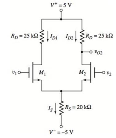
Given:
The given circuit is,
Calculation:
Consider the given figure,
Let calculate gate-to source voltage,
Now calculate source current,
Now find output voltage,
Hence,
b.
The differential-mode voltage gain and common-mode voltage gain along with CMRRdB
b.
Answer to Problem 11.46P
Explanation of Solution
Given:
The given circuit is,
Calculation:
Consider the small − signal equivalent circuit.
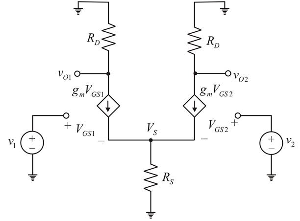
Apply KCL at node
Now,
Hence,
Want to see more full solutions like this?
Chapter 11 Solutions
MICROELECT. CIRCUIT ANALYSIS&DESIGN (LL)


- 2) The transistor parameters of the NMOS device in the common-gate amplifier in Figure 2 are VTN = 0.4V, K'n = 100 μA / V², and λ=0. (50 points) a) Find RD such that VDSQ = VDs (sat) + 0.25V. b) Determine the transistor W/L ratio such that the small-signal voltage gain is Av=6. c) What is the value of VGSQ? Сс 2 mA Rp T V=-1.8 V V+= 1.8 V Figure 2arrow_forwardCalculate the percent voltage regulation for a three-phase wye-connected 2500 kVA 6600-V turboalternator operating at full-load Unity power factor The per phase synchronous reactance and the armature resistance are 10.4 2 and 0.071 ≤2, respectively?arrow_forwardDon't use ai to answer I will report you answerarrow_forward
- Chose the correct answer: 1- A squirrel cage induction motor is not selected when (A) initial cost is the main consideration (B) maintenance cost is to be kept low (C) higher starting torque is the main consideration (D) all above considerations are involved 2- The torque of an induction motor is .............. (A) directly proportional to slip (B) inversely proportional to slip... (C) proportional to the square of the slip (D) none of the above 3- Insertion of resistance in the stator of an induction motor. (A) increases the load torque (B) decreases the starting torque (C) increases the starting torque (D) none of above tool to slip 10 or of the above 4- Increase in the length of air-gap in the induction motor results in the increasing of its (A) air-gap flux (B) magnetizing current (C) speed (D) power factor 5- In cumulatively cascade method for speed controlling, if PA is the number of poles of main motor and PB is the number of poles of auxiliary motor. Then the speed of the set…arrow_forwardChose the correct answer: 1- The resultant flux in stator winding of three-phase induction motor is equal to (A) Maximum value of flux due to any phase (B) Twice of the maximum value of flux due to any phase. (C) 0.5 times the maximum value of flux due to any phase (D) 1.5 times the maximum value of flux due to any phase 2- Which one of the following starters cannot be used for 3-phase, star - connected, slip-ring induction motor? (A) Auto-transformer starter (B) Star-delta starter (C) Direct-on-line starter (D) Rotor resistance starter 3- The crawling in the induction motor is caused by.............. (A) low voltage supply (B) high loads (D) improper design of the machine (C) harmonics developed in the motor 4- The 'cogging' of an induction motor can be avoided by........... (A) good ventilation (B) using DOL starter (C) star-connecting of stator winding (D) having number of rotor slots more or less than the number of stator slots 5- The method which can be used for the speed control…arrow_forwardManual solution only, no Al usedarrow_forward
 Power System Analysis and Design (MindTap Course ...Electrical EngineeringISBN:9781305632134Author:J. Duncan Glover, Thomas Overbye, Mulukutla S. SarmaPublisher:Cengage Learning