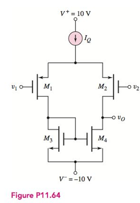
The differential amplifier in Figure P11.64 has a pair of PMOS transistors as input devices and a pair of NMOS transistors connected as an active load. The circuit is biased with I Q = 0.2 mA , and the transistor parameters are: K n = K p = 0.1 mA / V 2 , λ n = 0.01 V − 1 , λ p = 0.015 V − 1 V T N = 1 V , and V T P = − 1 V . (a) Determine the quiescent drain-to source voltage in each transistor. (b) Find the open-circuit differential mode voltage gain. (c) What is the output resistance?
The differential amplifier in Figure P11.64 has a pair of PMOS transistors as input devices and a pair of NMOS transistors connected as an active load. The circuit is biased with I Q = 0.2 mA , and the transistor parameters are: K n = K p = 0.1 mA / V 2 , λ n = 0.01 V − 1 , λ p = 0.015 V − 1 V T N = 1 V , and V T P = − 1 V . (a) Determine the quiescent drain-to source voltage in each transistor. (b) Find the open-circuit differential mode voltage gain. (c) What is the output resistance?
Solution Summary: The diagram shows the value of the quiescent drain to source voltage in each transistor.
The differential amplifier in Figure P11.64 has a pair of PMOS transistors as input devices and a pair of NMOS transistors connected as an active load. The circuit is biased with
I
Q
=
0.2
mA
,
and the transistor parameters are:
K
n
=
K
p
=
0.1
mA
/
V
2
,
λ
n
=
0.01
V
−
1
,
λ
p
=
0.015
V
−
1
V
T
N
=
1
V
,
and
V
T
P
=
−
1
V
.
(a) Determine the quiescent drain-to source voltage in each transistor. (b) Find the open-circuit differential mode voltage gain. (c) What is the output resistance?
A dc compound motor having a rating of 10 kW,
1150 r/min, 230 V, 50 A, has the following losses at
full-load:
bearing friction loss
40 W
brush friction loss
==
50 W
windage loss
=
200 W
(1)
total mechanical losses
=
290 W
(2)
iron losses
=
420 W
(3)
copper loss in the shunt field
=
120 W
copper losses at full-load:
(4)
a. in the armature
b. in the series field
c. in the commutating winding
total copper loss in the
500 W
25 W
70 W
armature circuit at full-load
=
595 W
4 What determines the power rating of a ma-
chine?
-5 If we cover up the vents in a motor, its out-
put power must be reduced. Explain.
-6 If a motor operates in a cold environment,
may we load it above its rated power? Why?
An electric motor driving a skip hoist with-
draws 1.5 metric tons of minerals from a
trench 20 m deep every 30 seconds. If the
hoist has an overall efficiency of 94 percent,
calculate the power output of the motor in
horsepower and in kilowatts.
Need a deep-dive on the concept behind this application? Look no further. Learn more about this topic, electrical-engineering and related others by exploring similar questions and additional content below.


 Introductory Circuit Analysis (13th Edition)Electrical EngineeringISBN:9780133923605Author:Robert L. BoylestadPublisher:PEARSON
 Delmar's Standard Textbook Of ElectricityElectrical EngineeringISBN:9781337900348Author:Stephen L. HermanPublisher:Cengage Learning
 Programmable Logic ControllersElectrical EngineeringISBN:9780073373843Author:Frank D. PetruzellaPublisher:McGraw-Hill Education
 Fundamentals of Electric CircuitsElectrical EngineeringISBN:9780078028229Author:Charles K Alexander, Matthew SadikuPublisher:McGraw-Hill Education
 Electric Circuits. (11th Edition)Electrical EngineeringISBN:9780134746968Author:James W. Nilsson, Susan RiedelPublisher:PEARSON
 Engineering ElectromagneticsElectrical EngineeringISBN:9780078028151Author:Hayt, William H. (william Hart), Jr, BUCK, John A.Publisher:Mcgraw-hill Education,