Microelectronics: Circuit Analysis and Design
4th Edition
ISBN: 9780073380643
Author: Donald A. Neamen
Publisher: McGraw-Hill Companies, The
bartleby

Concept explainers

bartleby

Videos

Textbook Question
Book Icon
Chapter 11, Problem 11.1EP

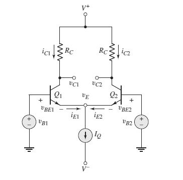
The circuit parameters for the differential amplifier shown in Figure 11.2 are V + = 5 V , V = 5 V , I Q = 0.3 mA , and R C = 20 k Ω . The transistor Parameters are β = 180 , V B E ( on ) = 0.7 V , and V A = . Determine the voltages v E , v C 1 , v C 2 , v C E 1 , and v C E 2 for ( a ) v 1 = v 2 = 0 , ( b ) v 1 = v 2 = 1 V and (c) v 1 = v 2 = + 1 V. (Ans. (a) v E = 0.7 V , v C 1 = v C 2 = 2 V , v C E 1 = v C E 2 = 2.7 V ; (b) v E = 1.7 V , v C 1 = v C 2 = 2 V , v C E 1 = v C E 2 = 3.7 V (c) v E = + 0.3 V , v C 1 = v C 2 = 2 V , v C E 1 = v C E 2 = 1.7 V ) .

a.

Expert Solution
Check Mark
To determine

The collector voltages, collector to emitter voltages and the emitter voltage for the given input values of a differential amplifier.

Answer to Problem 11.1EP

  vE=0.7 V , vC1=2 V  , vC2=2 V , vCE1=2.7 V , vCE2=2.7 V

Explanation of Solution

Given Information:

The given values are:

  V+=5 V, V=5 V,IQ=0.3 mA,RC=20 kΩ,β=180,VBE(on)=0.7 V,VA=v1=v2=0

The given circuit is shown below.

  Microelectronics: Circuit Analysis and Design, Chapter 11, Problem 11.1EP , additional homework tip  1

Calculation:

Voltage at emitter of each transistor

  vE=0VBE(on)

  vE=0.7 V

Assume transistors are matched. Then,

  iE1=iE2=IQ2

Also assume that the bias currents are negligible. Then,

  iC1iE1=IQ2,iC2=iE2=IQ2

Now

  vC1=vC2=V+IQ2RC=50.15×20 V

  vC1=2 V, vC2=2 V

Then,

  vCE1=vC1vE=2(0.7)

  vCE1=2.7 V

Similarly,

  vCE2=vC2vE=2(0.7)

  vCE2=2.7 V

b.

Expert Solution
Check Mark
To determine

The collector voltages, collector to emitter voltages and the emitter voltage for the given values of a differential amplifier.

Answer to Problem 11.1EP

  vE=1.7 V , vC1=2 V  , vC2=2 V , vCE1=3.7 V , vCE2=3.7 V

Explanation of Solution

Given Information:

The given values are:

  V+=5 V, V=5 V,IQ=0.3 mA,RC=20 kΩ,β=180,VBE(on)=0.7 V,VA=v1=v2=1 V

The given circuit is shown below.

  Microelectronics: Circuit Analysis and Design, Chapter 11, Problem 11.1EP , additional homework tip  2

Calculation:

Voltage at emitter of each transistor

  vE=v1VBE(on)=10.7 V

  vE=1.7 V

Assume transistors are matched. Then,

  iE1=iE2=IQ2

Also assume the bias currents are negligible. Then,

  iC1iE1=IQ2,iC2iE2=IQ2

Now

  vC1=vC2=V+IQ2RC=50.15×20 V

  vC1=2 V, vC2=2 V

Then,

  vCE1=vC1vE=2(1.7)

  vCE1=3.7 V

Similarly,

  vCE2=vC2vE=2(0.7)

  vCE2=3.7 V

c.

Expert Solution
Check Mark
To determine

The collector voltages, collector to emitter voltages and the emitter voltage for the given values of differential amplifier.

Answer to Problem 11.1EP

  vE=0.3 V , vC1=2 V  , vC2=2 V , vCE1=1.7 V , vCE2=1.7 V

Explanation of Solution

Given Information:

The given values are:

  V+=5 V, V=5 V,IQ=0.3 mA,RC=20 kΩ,β=180,VBE(on)=0.7 V,VA=v1=v2=+1 V

The given circuit is shown below.

  Microelectronics: Circuit Analysis and Design, Chapter 11, Problem 11.1EP , additional homework tip  3

Calculation:

Voltage at emitter of each transistor

  vE=v1VBE(on)=10.7 V

  vE=0.3 V

Assume transistors are matched. Then,

  iE1=iE2=IQ2

Also assume the bias currents are negligible. Then,

  iC1iE1=IQ2,iC2iE2=IQ2

Now

  vC1=vC2=V+IQ2RC=50.15×20 V

  vC1=2 V, vC2=2 V

Then,

  vCE1=vC1vE=2(0.3)

  vCE1=1.7 V

Similarly,

  vCE2=vC2vE=2(0.3)

  vCE2=1.7 V

Want to see more full solutions like this?

Subscribe now to access step-by-step solutions to millions of textbook problems written by subject matter experts!
Students have asked these similar questions
A singl core cable of voltage 30 kv. The diameter of Conductor is 3 cm. The diameter of cable is 25 cm. This cable has Two layer of insulator having arelative permittivity 5-3 respectively of The ratio of maximum electric stress of maximum electric stress 8 First layer to the of second layer is 10 Find & 1- The thickness of each layers. 3- The voltage of each layers. §. Layers The saving in radius of cable if another ungrading cable has the Same maximum electric stress, Total village, Conductor diameter of grading cable.
66 KV sing care Cable has a drameter of conductor of 3 cm. The radius of cable is 10 cm. This Cable house Two relative permmitivity of insulation 6 and 4 respectively. If The ratio of maximum electric stress of first layer to the maximum eledric streep & second layer is s 1- find the village & each layers. 2- Min- electric stress J Cable 3- Compare the voltage of ungrading Cable has the same distance and relectric stresses.
Prelab Information 1. Laboratory Preliminary Discussion First-order Low-pass RC Filter Analysis The first-order low-pass RC filter shown in figure 1 below represents all voltages and currents in the time domain. It is of course possible to solve for all circuit voltages using time domain differential equation techniques, but it is more efficient to convert the circuit to its s-domain equivalent as shown in figure 2 and apply Laplace transform techniques. vs(t) i₁(t) + R₁ ww V₁(t) 12(t) Lic(t) Vout(t) = V2(t) R₂ Vc(t) C Vc(t) VR2(t) = V2(t) + Vs(s) Figure 1: A first-order low-pass RC filter represented in the time domain. I₁(s) R1 W + V₁(s) V₂(s) 12(s) Ic(s) + Vout(S) == Vc(s) Vc(s) Zc(s) = = VR2(S) V2(s) Figure 2: A first-order low-pass RC filter represented in the s-domain.

Chapter 11 Solutions

Microelectronics: Circuit Analysis and Design

Ch. 11 - Prob. 11.7EPCh. 11 - Prob. 11.4TYUCh. 11 - Prob. 11.5TYUCh. 11 - The parameters of the diff-amp shown in Figure...Ch. 11 - For the differential amplifier in Figure 11.20,...Ch. 11 - The parameters of the circuit shown in Figure...Ch. 11 - The circuit parameters of the diff-amp shown in...Ch. 11 - Consider the differential amplifier in Figure...Ch. 11 - The diff-amp in Figure 11.19 is biased at IQ=100A....Ch. 11 - Prob. 11.10TYUCh. 11 - The diff-amp circuit in Figure 11.30 is biased at...Ch. 11 - Prob. 11.11EPCh. 11 - Prob. 11.12EPCh. 11 - Prob. 11.11TYUCh. 11 - Prob. 11.12TYUCh. 11 - Redesign the circuit in Figure 11.30 using a...Ch. 11 - Prob. 11.14TYUCh. 11 - Prob. 11.15TYUCh. 11 - Prob. 11.16TYUCh. 11 - Prob. 11.17TYUCh. 11 - Consider the Darlington pair Q6 and Q7 in Figure...Ch. 11 - Prob. 11.14EPCh. 11 - Consider the Darlington pair and emitter-follower...Ch. 11 - Prob. 11.19TYUCh. 11 - Prob. 11.15EPCh. 11 - Consider the simple bipolar op-amp circuit in...Ch. 11 - Prob. 11.17EPCh. 11 - Define differential-mode and common-mode input...Ch. 11 - Prob. 2RQCh. 11 - From the dc transfer characteristics,...Ch. 11 - What is meant by matched transistors and why are...Ch. 11 - Prob. 5RQCh. 11 - Explain how a common-mode output signal is...Ch. 11 - Define the common-mode rejection ratio, CMRR. What...Ch. 11 - What design criteria will yield a large value of...Ch. 11 - Prob. 9RQCh. 11 - Define differential-mode and common-mode input...Ch. 11 - Sketch the de transfer characteristics of a MOSFET...Ch. 11 - Sketch and describe the advantages of a MOSFET...Ch. 11 - Prob. 13RQCh. 11 - Prob. 14RQCh. 11 - Describe the loading effects of connecting a...Ch. 11 - Prob. 16RQCh. 11 - Prob. 17RQCh. 11 - Prob. 18RQCh. 11 - (a) A differential-amplifier has a...Ch. 11 - Prob. 11.2PCh. 11 - Consider the differential amplifier shown in...Ch. 11 - Prob. 11.4PCh. 11 - Prob. D11.5PCh. 11 - The diff-amp in Figure 11.3 of the text has...Ch. 11 - The diff-amp configuration shown in Figure P11.7...Ch. 11 - Consider the circuit in Figure P11.8, with...Ch. 11 - The transistor parameters for the circuit in...Ch. 11 - Prob. 11.10PCh. 11 - Prob. 11.11PCh. 11 - The circuit and transistor parameters for the...Ch. 11 - Prob. 11.13PCh. 11 - Consider the differential amplifier shown in...Ch. 11 - Consider the circuit in Figure P11.15. The...Ch. 11 - Prob. 11.16PCh. 11 - Prob. 11.17PCh. 11 - For the diff-amp in Figure 11.2, determine the...Ch. 11 - Prob. 11.19PCh. 11 - Prob. D11.20PCh. 11 - Prob. 11.21PCh. 11 - The circuit parameters of the diff-amp shown in...Ch. 11 - Consider the circuit in Figure P11.23. Assume the...Ch. 11 - Prob. 11.24PCh. 11 - Consider the small-signal equivalent circuit of...Ch. 11 - Prob. D11.26PCh. 11 - Prob. 11.27PCh. 11 - A diff-amp is biased with a constant-current...Ch. 11 - The transistor parameters for the circuit shown in...Ch. 11 - Prob. D11.30PCh. 11 - For the differential amplifier in Figure P 11.31...Ch. 11 - Prob. 11.32PCh. 11 - Prob. 11.33PCh. 11 - Prob. 11.34PCh. 11 - Prob. 11.35PCh. 11 - Prob. 11.36PCh. 11 - Consider the normalized de transfer...Ch. 11 - Prob. 11.38PCh. 11 - Consider the circuit shown in Figure P 11.39 . The...Ch. 11 - Prob. 11.40PCh. 11 - Prob. 11.41PCh. 11 - Prob. 11.42PCh. 11 - Prob. 11.43PCh. 11 - Prob. D11.44PCh. 11 - Prob. D11.45PCh. 11 - Prob. 11.46PCh. 11 - Consider the circuit shown in Figure P 11.47 ....Ch. 11 - Prob. 11.48PCh. 11 - Prob. 11.49PCh. 11 - Prob. 11.50PCh. 11 - Consider the MOSFET diff-amp with the...Ch. 11 - Consider the bridge circuit and diff-amp described...Ch. 11 - Prob. D11.53PCh. 11 - Prob. 11.54PCh. 11 - Prob. 11.55PCh. 11 - Consider the JFET diff-amp shown in Figure P11.56....Ch. 11 - Prob. 11.57PCh. 11 - Prob. 11.58PCh. 11 - Prob. D11.59PCh. 11 - The differential amplifier shown in Figure P 11.60...Ch. 11 - Prob. 11.61PCh. 11 - Consider the diff-amp shown in Figure P 11.62 ....Ch. 11 - Prob. 11.63PCh. 11 - The differential amplifier in Figure P11.64 has a...Ch. 11 - Prob. 11.65PCh. 11 - Consider the diff-amp with active load in Figure...Ch. 11 - The diff-amp in Figure P 11.67 has a...Ch. 11 - Consider the diff-amp in Figure P11.68. The PMOS...Ch. 11 - Prob. 11.69PCh. 11 - Prob. 11.70PCh. 11 - Prob. D11.71PCh. 11 - Prob. D11.72PCh. 11 - An all-CMOS diff-amp, including the current source...Ch. 11 - Prob. D11.74PCh. 11 - Consider the fully cascoded diff-amp in Figure...Ch. 11 - Consider the diff-amp that was shown in Figure...Ch. 11 - Prob. 11.77PCh. 11 - Prob. 11.78PCh. 11 - Prob. 11.79PCh. 11 - Prob. 11.80PCh. 11 - Consider the BiCMOS diff-amp in Figure 11.44 ,...Ch. 11 - The BiCMOS circuit shown in Figure P11.82 is...Ch. 11 - Prob. 11.83PCh. 11 - Prob. 11.84PCh. 11 - For the circuit shown in Figure P11.85, determine...Ch. 11 - The output stage in the circuit shown in Figure P...Ch. 11 - Prob. 11.87PCh. 11 - Consider the circuit in Figure P11.88. The bias...Ch. 11 - Prob. 11.89PCh. 11 - Consider the multistage bipolar circuit in Figure...Ch. 11 - Prob. D11.91PCh. 11 - Prob. 11.92PCh. 11 - For the transistors in the circuit in Figure...Ch. 11 - Prob. 11.94PCh. 11 - Prob. 11.95PCh. 11 - Prob. 11.96PCh. 11 - Consider the diff-amp in Figure 11.55 . The...Ch. 11 - The transistor parameters for the circuit in...
Knowledge Booster
Background pattern image
Electrical Engineering
Learn more about
Need a deep-dive on the concept behind this application? Look no further. Learn more about this topic, electrical-engineering and related others by exploring similar questions and additional content below.
Similar questions
SEE MORE QUESTIONS
Recommended textbooks for you
Text book image
Introductory Circuit Analysis (13th Edition)
Electrical Engineering
ISBN:9780133923605
Author:Robert L. Boylestad
Publisher:PEARSON
Text book image
Delmar's Standard Textbook Of Electricity
Electrical Engineering
ISBN:9781337900348
Author:Stephen L. Herman
Publisher:Cengage Learning
Text book image
Programmable Logic Controllers
Electrical Engineering
ISBN:9780073373843
Author:Frank D. Petruzella
Publisher:McGraw-Hill Education
Text book image
Fundamentals of Electric Circuits
Electrical Engineering
ISBN:9780078028229
Author:Charles K Alexander, Matthew Sadiku
Publisher:McGraw-Hill Education
Text book image
Electric Circuits. (11th Edition)
Electrical Engineering
ISBN:9780134746968
Author:James W. Nilsson, Susan Riedel
Publisher:PEARSON
Text book image
Engineering Electromagnetics
Electrical Engineering
ISBN:9780078028151
Author:Hayt, William H. (william Hart), Jr, BUCK, John A.
Publisher:Mcgraw-hill Education,
What is a Power Amplifier, And Do I Need One?; Author: Sweetwater;https://www.youtube.com/watch?v=2wkmSm4V00M;License: Standard Youtube License