Microelectronics: Circuit Analysis and Design
4th Edition
ISBN: 9780073380643
Author: Donald A. Neamen
Publisher: McGraw-Hill Companies, The
expand_more
expand_more
format_list_bulleted
Concept explainers
Textbook Question
Chapter 1, Problem 1.40P
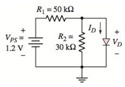
The diode in the circuit shown in Figure P1.40 has a reverse−saturation current of

Figure P1.40
Expert Solution & Answer
Want to see the full answer?
Check out a sample textbook solution
Students have asked these similar questions
Solve by hand do not use chatgpt or AI otherwise downvote
Don't use ai to answer I will report you answer
Not use ai please
Chapter 1 Solutions
Microelectronics: Circuit Analysis and Design
Ch. 1 - Calculate the intrinsic carrier concentration in...Ch. 1 - (a) Calculate the majority and minority carrier...Ch. 1 - Consider ntype GaAs at T=300K doped to a...Ch. 1 - Consider silicon at T=300K . Assume the hole...Ch. 1 - Determine the intrinsic carrier concentration in...Ch. 1 - (a) Consider silicon at T=300K . Assume that...Ch. 1 - Using the results of TYU1.2, determine the drift...Ch. 1 - The electron and hole diffusion coefficients in...Ch. 1 - A sample of silicon at T=300K is doped to...Ch. 1 - (a) Calculate Vbi for a GaAs pn junction at T=300K...
Ch. 1 - A silicon pn junction at T=300K is doped at...Ch. 1 - (a) A silicon pn junction at T=300K has a...Ch. 1 - (a) Determine Vbi for a silicon pn junction at...Ch. 1 - A silicon pn junction diode at T=300K has a...Ch. 1 - Recall that the forwardbias diode voltage...Ch. 1 - Consider the circuit in Figure 1.28. Let VPS=4V ,...Ch. 1 - (a) Consider the circuit shown in Figure 1.28. Let...Ch. 1 - The resistor parameter in the circuit shown in...Ch. 1 - Consider the diode and circuit in Exercise EX 1.8....Ch. 1 - Consider the circuit in Figure 1.28. Let R=4k and...Ch. 1 - The power supply (input) voltage in the circuit of...Ch. 1 - (a) The circuit and diode parameters for the...Ch. 1 - Determine the diffusion conductance of a pn...Ch. 1 - Determine the smallsignal diffusion resistance of...Ch. 1 - The diffusion resistance of a pn junction diode at...Ch. 1 - A pn junction diode and a Schottky diode both have...Ch. 1 - Consider the circuit shown in Figure 1.45....Ch. 1 - Consider the circuit shown in Figure 1.46. The...Ch. 1 - A Zener diode has an equivalent series resistance...Ch. 1 - The resistor in the circuit shown in Figure 1.45...Ch. 1 - Describe an intrinsic semiconductor material. What...Ch. 1 - Describe the concept of an electron and a hole as...Ch. 1 - Describe an extrinsic semiconductor material. What...Ch. 1 - Describe the concepts of drift current and...Ch. 1 - How is a pn junction formed? What is meant by a...Ch. 1 - How is a junction capacitance created in a...Ch. 1 - Write the ideal diode currentvoltage relationship....Ch. 1 - Describe the iteration method of analysis and when...Ch. 1 - Describe the piecewise linear model of a diode and...Ch. 1 - Define a load line in a simple diode circuit.Ch. 1 - Under what conditions is the smallsignal model of...Ch. 1 - Describe the operation of a simple solar cell...Ch. 1 - How do the i characteristics of a Schottky barrier...Ch. 1 - What characteristic of a Zener diode is used in...Ch. 1 - Describe the characteristics of a photodiode and a...Ch. 1 - (a) Calculate the intrinsic carrier concentration...Ch. 1 - (a) The intrinsic carrier concentration in silicon...Ch. 1 - Calculate the intrinsic carrier concentration in...Ch. 1 - (a) Find the concentration of electrons and holes...Ch. 1 - Gallium arsenide is doped with acceptor impurity...Ch. 1 - Silicon is doped with 51016 arsenic atoms/cm3 ....Ch. 1 - (a) Calculate the concentration of electrons and...Ch. 1 - A silicon sample is fabricated such that the hole...Ch. 1 - The electron concentration in silicon at T=300K is...Ch. 1 - (a) A silicon semiconductor material is to be...Ch. 1 - (a) The applied electric field in ptype silicon is...Ch. 1 - A drift current density of 120A/cm2 is established...Ch. 1 - An ntype silicon material has a resistivity of...Ch. 1 - (a) The applied conductivity of a silicon material...Ch. 1 - In GaAs, the mobilities are n=8500cm2/Vs and...Ch. 1 - The electron and hole concentrations in a sample...Ch. 1 - The hole concentration in silicon is given by...Ch. 1 - GaAs is doped to Na=1017cm3 . (a) Calculate no and...Ch. 1 - (a) Determine the builtin potential barrier Vbi in...Ch. 1 - Consider a silicon pn junction. The nregion is...Ch. 1 - The donor concentration in the nregion of a...Ch. 1 - Consider a uniformly doped GaAs pn junction with...Ch. 1 - The zerobiased junction capacitance of a silicon...Ch. 1 - The zerobias capacitance of a silicon pn junction...Ch. 1 - The doping concentrations in a silicon pn junction...Ch. 1 - (a) At what reversebias voltage does the...Ch. 1 - (a) The reversesaturation current of a pn junction...Ch. 1 - (a) The reversesaturation current of a pn junction...Ch. 1 - A silicon pn junction diode has an emission...Ch. 1 - Plot log10ID versus VD over the range 0.1VD0.7V...Ch. 1 - (a) Consider a silicon pn junction diode operating...Ch. 1 - A pn junction diode has IS=2nA . (a) Determine the...Ch. 1 - The reversebias saturation current for a set of...Ch. 1 - A germanium pn junction has a diode current of...Ch. 1 - (a)The reversesaturation current of a gallium...Ch. 1 - The reversesaturation current of a silicon pn...Ch. 1 - A silicon pn junction diode has an applied...Ch. 1 - A pn junction diode is in series with a 1M...Ch. 1 - Consider the diode circuit shown in Figure P1.39....Ch. 1 - The diode in the circuit shown in Figure P1.40 has...Ch. 1 - Prob. 1.41PCh. 1 - (a) The reversesaturation current of each diode in...Ch. 1 - (a) Consider the circuit shown in Figure P1.40....Ch. 1 - Consider the circuit shown in Figure P1.44....Ch. 1 - The cutin voltage of the diode shown in the...Ch. 1 - Find I and VO in each circuit shown in Figure...Ch. 1 - Repeat Problem 1.47 if the reversesaturation...Ch. 1 - (a) In the circuit Shown in Figure P1.49, find the...Ch. 1 - Assume each diode in the circuit shown in Figure...Ch. 1 - (a) Consider a pn junction diode biased at IDQ=1mA...Ch. 1 - Determine the smallsignal diffusion resistancefor...Ch. 1 - The diode in the circuit shown in Figure P1.53 is...Ch. 1 - The forwardbias currents in a pn junction diode...Ch. 1 - A pn junction diode and a Schottky diode have...Ch. 1 - The reversesaturation currents of a Schottky diode...Ch. 1 - Consider the Zener diode circuit shown in Figure...Ch. 1 - (a) The Zener diode in Figure P1.57 is ideal with...Ch. 1 - Consider the Zener diode circuit shown in Figure...Ch. 1 - The Output current of a pn junction diode used as...Ch. 1 - Using the currentvoltage characteristics of the...Ch. 1 - (a) Using the currentvoltage characteristics of...Ch. 1 - Use a computer simulation to generate the ideal...Ch. 1 - Use a computer simulation to find the diode...Ch. 1 - Design a diode circuit to produce the load line...Ch. 1 - Design a circuit to produce the characteristics...Ch. 1 - Design a circuit to produce the characteristics...Ch. 1 - Design a circuit to produce the characteristics...
Knowledge Booster
Learn more about
Need a deep-dive on the concept behind this application? Look no further. Learn more about this topic, electrical-engineering and related others by exploring similar questions and additional content below.Similar questions
- 49. For the circuit below, what is the best connection of the capacitor to filte voltage? ბი DO A O BO wwwww wwwww M m H E LOADarrow_forward5.25. Determine the corner frequency resulting from Cin in Fig. 5.47(d). For simplicity, assume C₁ is a short circuit. TVDD C₁ M2 RF Vin H w - Vout Cin M₁arrow_forwardIn the below circuit, find out the value of equivalent Thevenin's voltage and Thevenin's resistance at the terminal. 2000 0.25 A 400 2 800 2 0.1 Aarrow_forward
- Q1: For the circuit shown in Figure-1, (a) Calculate the equivalent resistance of the circuit, RAB at the terminals A and B. [10] (b) When 50V dc source is switched at terminals A-B, solve for the voltage V₁ at the location shown. [10] 50V www 12Ω 10Ω 5Ω www www A + B 200 Figure-1 www 10Ω ww 25Ω 100arrow_forwarda. Write a PLC ladder diagram that allows the teacher to teach AND, OR, and XOR logic gates through using three PLC's digital input points and only one digital output point.arrow_forwardrately by PRACTICE 4.2 For the circuit of Fig. 4.5, compute the voltage across each curren source. 202 ww 3A 30 ww 4Ω S 50 www Reference node FIGURE 4.5 Ans: V3A =5.235 V; 7A = 11.47 V. 7 Aarrow_forward
- Q2) a) design and show me your steps to convert the following signal from continuous form to digital form: s(t)=3sin(3πt) -1 373 Colesarrow_forwardA sequence is defined by the relationship r[n] = [h[m]h[n+m]=hn*h-n where h[n] is a minimum-phase sequence and r[n]= 4 4 (u[n]+ 12" [n-1] 3 (a) Find R(z) and sketch the pole-zero diagram. (b) Determine the minimum-phase sequence h[n] to within a scale factor of ±1. Also, determine the z-transform H(z) of h[n].arrow_forwardusıng j-k and D flipflop design a counter that counts 0,2,1 again as shown below ın the tablearrow_forward
- find the minterms of the followıng boolean expressıon desıgn F's cırcuit using one of the approciate decoders given below and a NOR gateF(A,B,C,D)=(A+'BC)(B 'C+'A 'D + CD)arrow_forward64) answer just two from three the following terms: A) Design ADC using the successive method if the Vmax=(3) volt, Vmin=(-2) volt, demonstrate the designing system for vin-1.2 volt. Successive Approximation ADC Input Voltage-1.1 V -4-3.5-3 -2.5 -2 -1.5 +1 -0.5 0 0.5 1 1.5 2 2.5 3 3.5 1 T -8 -7 -6 -5 -3 +2 -1 0 1 2 3 4 5 6 7 X=1??? 1st guess: -0.25 V (too high) X=11?? 2nd guess: -2.25 V (too low) 3rd guess: -1.25 V (too low) X=1110 X=111? 4th guess: -0.75 V (too high) Make successive guesses and use a comparator to tell whether your guess is too high or too low. Each guess determines one bit of the answer and cuts the number of remaining possibilities in half.arrow_forwardDatacommunıcatıonin a commuinaction ASYNCHRONOUS TRANSMİTİON is used in this transmistion 7-bit chatacter will be transfered even parity will be used ,stop element is as 1,5 bits a)=select a chracter yourself and dısplay the signal transfered in this transmission , and calculate the overhead in this transmisionarrow_forward
arrow_back_ios
SEE MORE QUESTIONS
arrow_forward_ios
Recommended textbooks for you

Diodes Explained - The basics how diodes work working principle pn junction; Author: The Engineering Mindset;https://www.youtube.com/watch?v=Fwj_d3uO5g8;License: Standard Youtube License