Concept explainers
Videos
(a)
The Thevenin equivalent resistance seen by the load resistor
Answer to Problem 3.60HP
The expression for the Thevenin resistance seen by the load resistor is
Explanation of Solution
Calculation:
The given diagram is shown in Figure 1
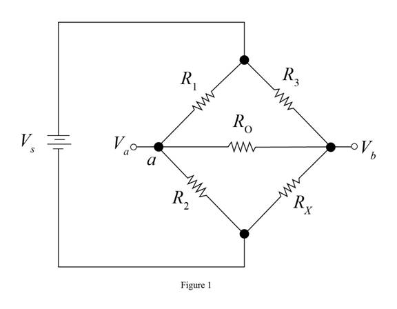
To calculate the Thevenin equivalent resistance, short circuit the voltage source and open circuit the load resistance, mark the values and redraw the circuit.
The required diagram is shown in Figure 2
From the above figure, the Thevenin equivalent resistance of the circuit is evaluated as,
Conclusion:
Therefore, the expression for the Thevenin resistance seen by the load resistor is
(b)
The Thevenin equivalent network seen by
Answer to Problem 3.60HP
The Thevenin equivalent circuit seen by the load is shown in Figure 4 and the power dissipated by the resistance
Explanation of Solution
Calculation:
The conversion of
The conversion of
Substitute
The expression for the Thevenin equivalent resistance is given by,
Substitute
The conversion of
The conversion of
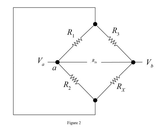
To calculate the Thevenin voltage open circuit the load resistance, mark the values and redraw the circuit.
The required diagram is shown in Figure 3
From the above figure the Thevenin equivalent voltage is calculated as,
Mark the values and draw the Thevenin equivalent circuit.
The required diagram is shown in Figure 4
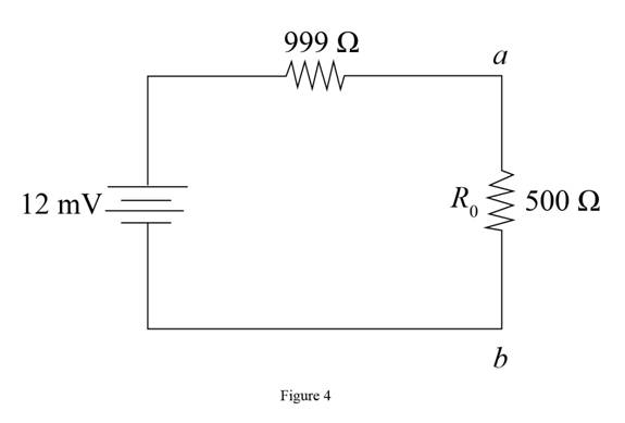
From Figure 4 the current that flows through the resistance of
The conversion of
The conversion of
The expression for the power dissipated by the load is given by,
Substitute
Conclusion:
Therefore, the Thevenin equivalent circuit seen by the load is shown in Figure 4 and the power dissipated by the resistance
(c)
The power dissipated by the Thevenin equivalent resistance seen by
Answer to Problem 3.60HP
The power dissipated by the resistance
Explanation of Solution
Calculation:
The expression to calculate the power dissipated by the Thevenin resistance of the circuit is given by,
Substitute
Conclusion:
Therefore, the power dissipated by the resistance
(d)
The power dissipated by the entire bridge when
Answer to Problem 3.60HP
The total power dissipated in the bridge is
Explanation of Solution
Calculation:
Redraw the circuit for the resistance
The required diagram is shown in Figure 5
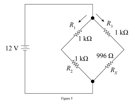
The current through the resistance
The expression for the power dissipated by the resistance is given by,
Substitute
The current through the resistance
The expression for the power dissipated by the resistance
Substitute
The current through the resistance
The expression for the power dissipated by the resistance
Substitute
The expression for the power dissipated by the resistance
Substitute
The expression for the total power dissipated by the bridge is given by,
Substitute
Conclusion:
Therefore, the total power dissipated in the bridge is
Want to see more full solutions like this?
Chapter 3 Solutions
Principles and Applications of Electrical Engineering


- What happens to the rotor speed and rotor current when the mechanical load on an in- duction motor increases? Would you recommend using a 50 hp in- duction motor to drive a 10 hp load? Explain. Give two advantages of a wound-rotor mo- tor over a squirrel-cage motor. Both the voltage and frequency induced in the rotor of an induction motor decrease as the rotor speeds up. Explain.arrow_forwardPlease provide explainations and detailed working. thank youarrow_forwardPlease provide explainations and detailed working. thank youarrow_forward
- The excitation of a three-phase synchronous motor connected in parallel with a load of 500 kW operating at 0-85 p.f. lagging is adjusted to improve the overall p.f. of the system to 0.95 lagging. If the mechanical load on the motor is 120 kW, calculate the kVA input to the synchronous motor and its p.f.?arrow_forwardA domestic load of 2300 kW at 0.88 p.f lagging and a motors load of 3400 kW at 0.85 p.f lagging are supplied by two alternators operating in parallel. If one alternator is delivering a load of 3300 kW at 0.9 p.f lagging, what will be the output power and p.f of the other alternator?arrow_forwardDesign a bank of capacitors to provide 60V and 2kWh energy to capture and store regen breaking energy. Use commercial supercapacitor cells at 3V and 3600F. Capacitor voltage drops almost linearly during discharge and below half voltage maximum it doesn’t provide significant power. If we discharge a fully charged capacitor to its half voltage maximum, how much energy can be discharged compared to a full-discharged capacitor (show your calculation)?arrow_forward
- 8-1) similar to Lathi & Ding, Prob. P.5.1-2 The figure below shows the Fourier spectra of signals of g,(t) and g₁(t). Determine the Nyquist rate and the corresponding sampling interval for signals of g,(t), g,(t), g₁(1) - g¸(1), g¸³(t), and g₁(1)g₁(1). Hint: Use the frequency convolution and the width property of convolution. G₁(f) G₂(f) -8000 0 8000 f -20000 10 20000 farrow_forwardCalculate the approximate values of the starting current, full-load current, and no- load current of a 150 horsepower, 575 V, 3- phase induction motor.arrow_forwardCapacitor voltage drops almost linearly during discharge and below half voltage maximum it doesn’t provide significant power. If we discharge a fully charged capacitor to its half voltage maximum, how much energy can be discharged compared to a full-discharged capacitor (show your calculation)?arrow_forward
- Design a bank of capacitors to provide 60V and 2kWh energy to capture and store regen breaking energy. Use commercial supercapacitor cells at 3V and 3600F.arrow_forwardPlease explain in step by step detail how to answer and solve this problemarrow_forwardTwo loads connected in parallel are respectively 2 kW at a pf of 0.75 leading and 4 kW at a pf of 0.95 lagging. Calculate the pf of the combined two loads. Find the complex power supplied by the source. Hints: • • Since the two loads are parallel, the complex power, S, supplied by the source is S = S₁+ S₂ Calculate the complex powers, S₁ and S2, of each load (use power triangles) and add them to find the total S. Calculate 0 and obtain pf.arrow_forward
 Introductory Circuit Analysis (13th Edition)Electrical EngineeringISBN:9780133923605Author:Robert L. BoylestadPublisher:PEARSON
 Delmar's Standard Textbook Of ElectricityElectrical EngineeringISBN:9781337900348Author:Stephen L. HermanPublisher:Cengage Learning
 Programmable Logic ControllersElectrical EngineeringISBN:9780073373843Author:Frank D. PetruzellaPublisher:McGraw-Hill Education
 Fundamentals of Electric CircuitsElectrical EngineeringISBN:9780078028229Author:Charles K Alexander, Matthew SadikuPublisher:McGraw-Hill Education
 Electric Circuits. (11th Edition)Electrical EngineeringISBN:9780134746968Author:James W. Nilsson, Susan RiedelPublisher:PEARSON
 Engineering ElectromagneticsElectrical EngineeringISBN:9780078028151Author:Hayt, William H. (william Hart), Jr, BUCK, John A.Publisher:Mcgraw-hill Education,