
Videos
Consider the NMOS circuit shown in Figure 3.39. Plot the voltage transfer characteristics using a PSpice simulation. Use transistor parameters similar to those in Example 3.10. What are the values of
To plot: The voltage transfer characteristics using PSpice simulation.
To find: The value of output voltage for the given input voltage.
Answer to Problem 3.4CAE
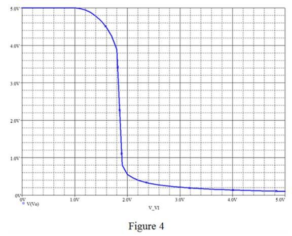
The required plot is shown in Figure 4 and the output voltage for the input voltage of
Explanation of Solution
Given:
The required diagram with the values marked is shown in Figure 1
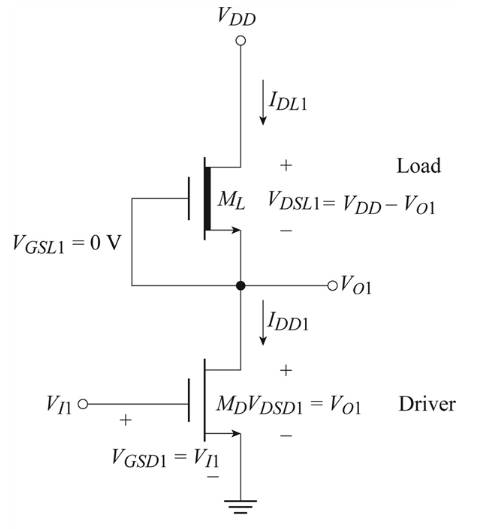
Figure 1
Calculation:
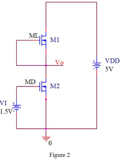
Draw the PSpice equivalent circuit with all the values marked.
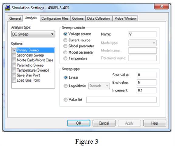
The snip for the drop box with all the setting is shown in Figure 3
Left click on the trace option and then click on add trace and type “V(Vo)”command in trace expression box to obtain the voltage transfer characteristic of the inverter.
The required characteristic diagram is shown in Figure 4
Consider the input voltage is
The expression for the current
The expression for the current
The expression for the value of the voltage
The expression for the current
Substitute
Substitute
Substitute
The input voltage is just
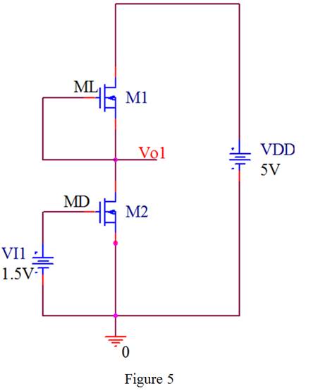
Draw the PSpice circuit for the figure 1 with the input voltage of
The required diagram is shown in Figure 5
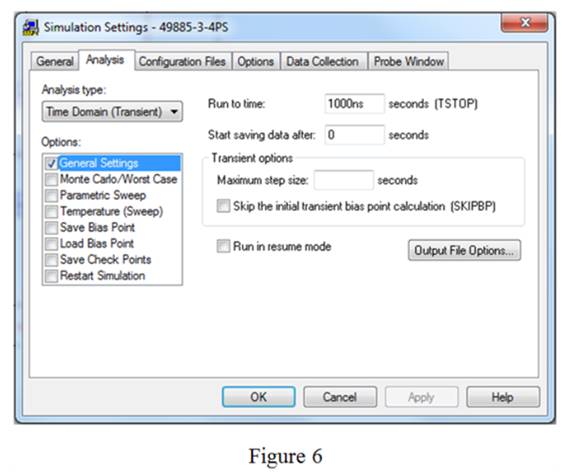
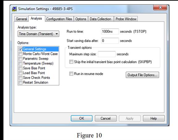
The simulation settings for the circuit is shown in Figure 6
The simulated circuit for Figure 5 with the output voltage is shown in Figure 7
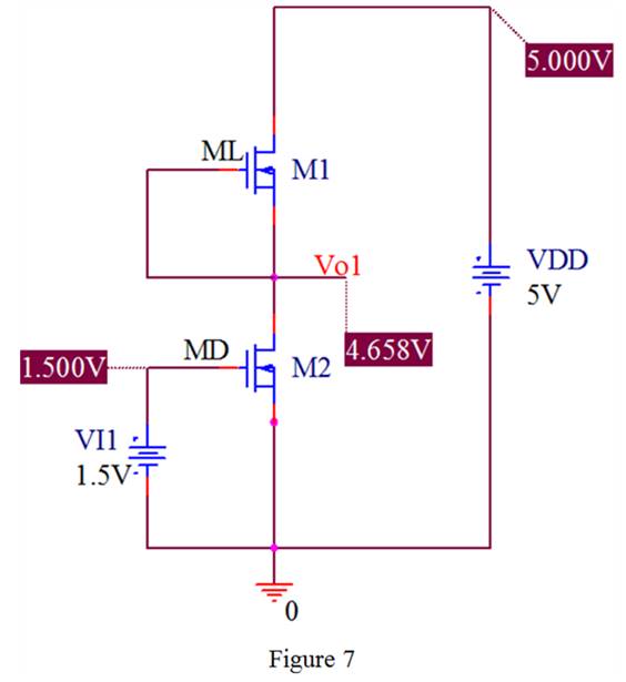
Thus, the value of the simulated output voltage is same as the theoretical output voltage.
Consider the input voltage is
Mark the values and draw the circuit for the input voltage of
The required diagram is shown in Figure 8
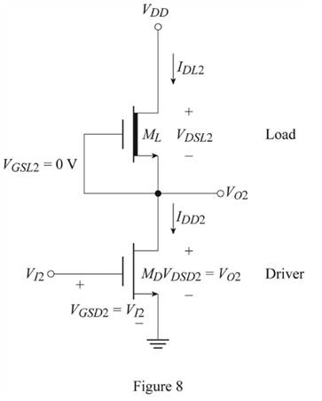
The values of different voltage are,
The driver transistor is biased in non-saturation region as the drain to source voltage is very large. So the expression for the relation of the drain currents is given by,
The expression for
The load transistor is in the saturation region and the drain current is given by,
By the relation
Substitute
The value of the output voltage is evaluated as,
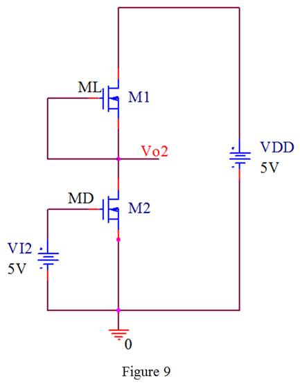
The simulation circuit for Figure 8 is shown in Figure 9
The output of the simulated circuit for the above circuit is shown in Figure 11
The circuit diagram with the output voltage is shown in Figure 11
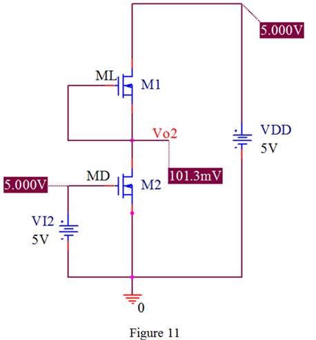
Thus, the output voltage of
Conclusion:
Therefore, the required plot is shown in Figure 4 and the output voltage for the input voltage of
Want to see more full solutions like this?
Chapter 3 Solutions
Microelectronics: Circuit Analysis and Design


- For the Circuit Below Find: A) io in terms of Rb and the numerical resistor values provided in the schematic. Reduce your solution to a minimal Equations B)the power delivered across Rb in terms of Rb and the numerical resistor values provided in the schematic. Reduce your solution to a minimal equation. C) the power delivered across Rc if Rb is 5 Q Ra $50 15Ω M 120 90V +1 Rb 150 150 m Rcarrow_forwardProblems A.1 The square-law modulator is a device for the generation of DSB-PC-AM signals. In the square-law modulator, the sum of the modulating signal and the carrier wave forms the input signal to a nonlinear device. The output signal of the nonlinear device is a linear combination of the input signal and the square of the input signal. The output signal of the nonlinear device is then band-pass filtered. The BPF has a center frequency that is the same as the carrier frequency and a bandwidth that is twice the message bandwidth. Show the output of the BPF is a DSB-PC-AM signal, and determine a requirement between the carrier frequency and the message bandwidth that must be satisfied.arrow_forwardGive the current voltage relationship of the D-MOSFET and E-MOSFET.arrow_forward
- Answer A is wrong.arrow_forwardThe part of machine level instruction, which tells the central processor what was to be done is: A. Address B. None of the above C. Operation code D. Operandarrow_forwardWhich of the following statement is TRUE? 1. In RISC processors, each instruction requires only two clock cycles to complete, resulting in consistent execution time 2. RISC has more transistors and fewer registers 3. RISC has more registers and fewer transistorsarrow_forward
- A half-wave controlled rectifier is supplied by a 230 Vrms voltage source and has load resistance of 2502. Calculate the delay angle a that produces a load-absorbed power of 200W.arrow_forwardnot use ai pleasearrow_forwardFigure 1 shows a half-wave controlled rectifier which is supplied by a Vin = 120 Vrms voltage source. Assume that the load resistance is R = 10 2. Determine: a) The firing angle a of the thyristor to produce an average output voltage 50Vdc. Vin=Vmsinoot b) The average power Po absorbed by the load R. Figure 1 R = 1092arrow_forward
 Introductory Circuit Analysis (13th Edition)Electrical EngineeringISBN:9780133923605Author:Robert L. BoylestadPublisher:PEARSON
 Delmar's Standard Textbook Of ElectricityElectrical EngineeringISBN:9781337900348Author:Stephen L. HermanPublisher:Cengage Learning
 Programmable Logic ControllersElectrical EngineeringISBN:9780073373843Author:Frank D. PetruzellaPublisher:McGraw-Hill Education
 Fundamentals of Electric CircuitsElectrical EngineeringISBN:9780078028229Author:Charles K Alexander, Matthew SadikuPublisher:McGraw-Hill Education
 Electric Circuits. (11th Edition)Electrical EngineeringISBN:9780134746968Author:James W. Nilsson, Susan RiedelPublisher:PEARSON
 Engineering ElectromagneticsElectrical EngineeringISBN:9780078028151Author:Hayt, William H. (william Hart), Jr, BUCK, John A.Publisher:Mcgraw-hill Education,