
Videos
Consider the NMOS circuit shown in Figure 3.36. Plot the voltage transfer characteristics, using a PSpice simulation. Use transistor parameters similar to those in Example 3.9. What are the values of
To plot: Thevoltage transfer characteristics using PSpice simulation.
To find: The value of output voltage for the given input voltage.
Answer to Problem 3.3CAE
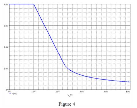
The required plot is shown in Figure 4 and the output voltage for the input voltage of
Explanation of Solution
Given:
The required diagram with the values marked is shown in Figure 1.
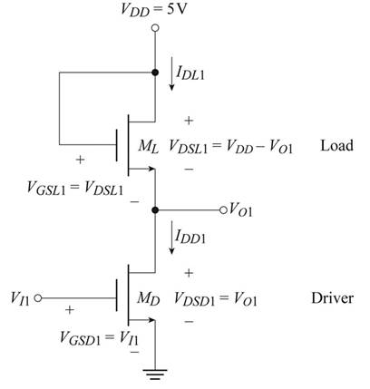
Figure 1
Calculation:
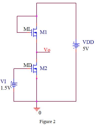
Draw the PSpice equivalent circuit with all the values marked.
The snip for the drop box with all the setting is shown in Figure 3

Left click on the trace option and then click on add trace and type “V(Vo)”command in trace expression box to obtain the voltage transfer characteristic of the inverter.
The required characteristic diagram is shown in Figure 4
Consider the input voltage is
The expression for the current
The expression for the current
The expression for the value of the voltage
The expression for the current
Substitute
Substitute
The input voltage is just
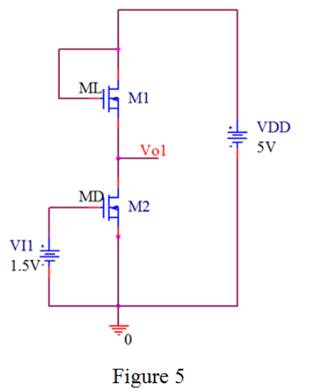
Draw the PSpice circuit for the figure 1 with the input voltage of
The required diagram is shown in Figure 5
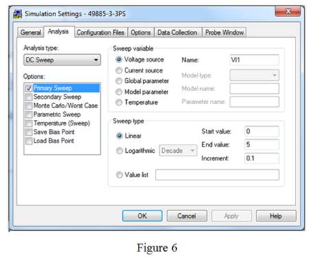
The simulation settings for the circuit is shown in Figure 6
The simulated circuit for Figure 5 with the output voltage is shown in Figure 7
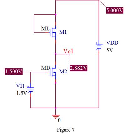
Thus, the value of the simulated output voltage is same as the theoretical output voltage.
Consider the input voltage is
Mark the values and draw the circuit for the input voltage of
The required diagram is shown in Figure 8
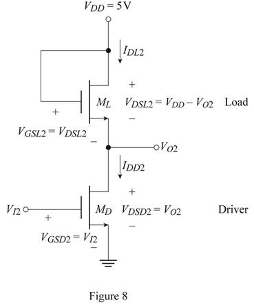
The values of different voltage are,
The driver transistor is biased in non-saturation region as the drain to source voltage is very large. So the expression for the relation of the drain currents is given by,
The expression for
The load transistor is in the saturation region and the drain current is given by,
By the relation
The value of the output voltage is evaluated as,
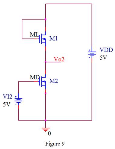
The simulation circuit for Figure 8 is shown in Figure 9
The output of the simulated circuit for the above circuit is shown in Figure 11
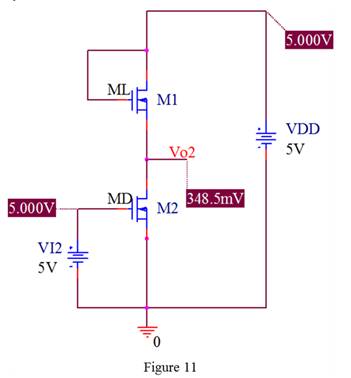
Thus, the output voltage of
Conclusion:
Therefore, the required plot is shown in Figure 4 and the output voltage for the input voltage of
Want to see more full solutions like this?
Chapter 3 Solutions
Microelectronics: Circuit Analysis and Design


- (a) For the circuit shown in Figure Q3(a) (RFC and Cc are forbias) (i) (ii) Draw the AC small signal equivalent circuit of the oscillator. From this equivalent circuit derive an equation for fo and the gain condition for the oscillations to start. VDD www RG eee RFC H Cc 北 5 C₁ L 000 C₂ Voarrow_forwardPlease solve this question step by step handwritten solution and do not use chat gpt or any ai toolsfor part ii) you may need to use nodal analysisarrow_forward12.1. Find the steady-state response vo (t) for the network. 00000- 1Ω ww 12 cos(t) V + www 202 1 H 202 1 F + 1Ω νο -arrow_forward
- A Three-phase, 12 pole, Y-connected alternator has 108 slots and 14 conductors per slot. The windings are (5/6 th) pitched. The flux per pole is 57 mWb distributed sinusoidally over the pole. If the machine runs at 500 r.p.m., determine the following: (a) The frequency of the generated e.m.f., (b) The distribution factor, (c) The pitch factor, and (d) The phase and line values of the generated e.m.f.?arrow_forwardTwo 3-ph, 6.6 kV, Y-connected, alternators supply a load of 3000 kW at 0.8 p.f. lagging. The synchronou impedance per phase of machine A is (0.5+110) and that of machine B is (0.4 +J12) . The excitation of machine A adjusted so that it delivers 150 A. The load is shared equally between the machines. Determine the armature curre p.f., induced e.m.f., and load angle of each machine?arrow_forwardName the circuit below? The output voltage is initially zero and the pulse width is 200 μs. Find the Vout and draw the output waveform? +2.5 V V 247 -2.5 V C 0.01 F Ri W 10 ΚΩarrow_forward
- Please work outarrow_forwardFind Vfinal when Vs up and Vs V. Which LED will light in each case? Red or Green? Justify your answers. Fill the table below. Vs 8 ΚΩ Vos Χρι + 3 ΚΩ www 6 ΚΩ ww 4 ΚΩ Yo www Vo Vec-12 V Nol V final Vm w 3 ΚΩ 5 V 38 ΚΩ R= 1 kQ V -12 V Red LED Green LED Vs Vo Vfinal Which LED is ON? Varrow_forwardCircuits help please solve and explain. Question in images providedarrow_forward
- + V 6.2 A 1.2 A S R 4 Ω Find the source voltage Vs 0.8 Aarrow_forwardDetermine i(t) for t≥ 0 given that the circuit below had been in steady state for a long time prior to t = 0. Also, I₁ = 1 5 A, R₁ =22, R2 =10 Q2, R3 = 32, R4 =7 2, and L=0.15 H. Also fill the table. m L ww R2 t = 0 R₁ 29 R3 R4 Time 0 iL(t) 0 8arrow_forwardPlease help explain this problemarrow_forward
 Introductory Circuit Analysis (13th Edition)Electrical EngineeringISBN:9780133923605Author:Robert L. BoylestadPublisher:PEARSON
 Delmar's Standard Textbook Of ElectricityElectrical EngineeringISBN:9781337900348Author:Stephen L. HermanPublisher:Cengage Learning
 Programmable Logic ControllersElectrical EngineeringISBN:9780073373843Author:Frank D. PetruzellaPublisher:McGraw-Hill Education
 Fundamentals of Electric CircuitsElectrical EngineeringISBN:9780078028229Author:Charles K Alexander, Matthew SadikuPublisher:McGraw-Hill Education
 Electric Circuits. (11th Edition)Electrical EngineeringISBN:9780134746968Author:James W. Nilsson, Susan RiedelPublisher:PEARSON
 Engineering ElectromagneticsElectrical EngineeringISBN:9780078028151Author:Hayt, William H. (william Hart), Jr, BUCK, John A.Publisher:Mcgraw-hill Education,