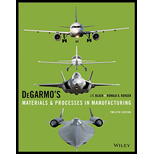
DeGarmo's Materials and Processes in Manufacturing
12th Edition
ISBN: 9781118987674
Author: J. T. Black, Ronald A. Kohser
Publisher: WILEY
expand_more
expand_more
format_list_bulleted
Textbook Question
Chapter 29, Problem 15RQ
What is the most complicated, expensive, and critical process in microelectronics?
Expert Solution & Answer
Want to see the full answer?
Check out a sample textbook solution
Students have asked these similar questions
Three cables are pulling on a ring located at the origin, as shown in the diagram below. FA is 200 N in magnitude with a transverse angle of 30° and an azimuth angle of 140°. FB is 240 N in magnitude with coordinate direction angles α = 135° and β = 45°. Determine the magnitude and direction of FC so that the resultant of all 3 force vectors lies on the z-axis and has a magnitude of 300 N. Specify the direction of FC using its coordinate direction angles.
turbomachienery
auto controls
Chapter 29 Solutions
DeGarmo's Materials and Processes in Manufacturing
Ch. 29 - Over the latter half of the 20th century, what...Ch. 29 - What was the major motivation for developing...Ch. 29 - Prob. 3RQCh. 29 - What is an example of a device feature that is...Ch. 29 - What type of manufacturing technology dominates...Ch. 29 - Name the four categories of miniature systems...Ch. 29 - Give two differences between lab-on-a-chip and...Ch. 29 - What is a scaling law?Ch. 29 - As the primary dimensions of an object decrease,...Ch. 29 - In the design of a water heater, the mean time...
Ch. 29 - Prob. 11RQCh. 29 - Name two conventional manufacturing processes that...Ch. 29 - Prob. 13RQCh. 29 - Why does breadth of scale of a product have an...Ch. 29 - What is the most complicated, expensive, and...Ch. 29 - Name three purposes that a resist mask can play.Ch. 29 - Name four key lithography methods.Ch. 29 - Name two through-mask lithography techniques.Ch. 29 - Name two direct-write lithography techniques.Ch. 29 - List the sequence of steps involved in...Ch. 29 - Of the two major classifications of photoresists,...Ch. 29 - List four requirements of a photoresist.Ch. 29 - What limits the resolution of a photoresist?Ch. 29 - What is meant by resist sensitivity?Ch. 29 - What is one requirement that contributes to the...Ch. 29 - List the three types of exposure methods used in...Ch. 29 - Why is projection printing equipment called a...Ch. 29 - What are typical materials etched during...Ch. 29 - What is etch bias?Ch. 29 - Prob. 30RQCh. 29 - What are some possible defects that can result...Ch. 29 - What are some possible defects that can result...Ch. 29 - List and describe two properties of etchants.Ch. 29 - What is etch anisotropy dependent upon?Ch. 29 - What is the difference between wet and dry?...Ch. 29 - What is dry etching?Ch. 29 - What are the three main categories of dry etching...Ch. 29 - What is the difference between plasma etching and...Ch. 29 - What is deep reactive ion etching?Ch. 29 - What is a benefit of using UV lasers to machine...Ch. 29 - Which type of non-lithographic micromachining...Ch. 29 - What are thin films?Ch. 29 - A) What is the difference between solution...Ch. 29 - What are the two broad categories of vapor...Ch. 29 - List two different types of physical vapor...Ch. 29 - List two advantages of sputtering over...Ch. 29 - What is meant by step coverage with regards to...Ch. 29 - Why is step coverage important?Ch. 29 - Prob. 49RQCh. 29 - What does gettering mean in relation to wafer...Ch. 29 - How are undesirable gas-phase reactions controlled...Ch. 29 - What is the key difference in the reactor designs...Ch. 29 - What are the two types of LPCVD reactor designs?...Ch. 29 - In metallization, what is the difference between a...Ch. 29 - What is the advantage of using plasma-enhanced on...Ch. 29 - A) What is epitaxy? B) is it important for...Ch. 29 - Name four techniques for solution deposition onto...Ch. 29 - Name four roll-to-roll processing techniques for...Ch. 29 - What is a semiconductor?Ch. 29 - Name three common semiconductor materials.Ch. 29 - Give three reasons why silicon is the most popular...Ch. 29 - Prob. 62RQCh. 29 - What is a silicon boule?Ch. 29 - Prob. 64RQCh. 29 - What are some geometric concerns involved with...Ch. 29 - What is meant by the term doping?Ch. 29 - What is the difference between n�type and...Ch. 29 - Name three methods for doping a silicon wafer.Ch. 29 - Prob. 69RQCh. 29 - Prob. 70RQCh. 29 - Prob. 71RQCh. 29 - Why are rapid thermal processing technologies...Ch. 29 - What are two ways in which silicon dioxide is...Ch. 29 - Give two reasons why wet oxidation is better...Ch. 29 - What is a p�n junction? \What can it be used...Ch. 29 - Prob. 76RQCh. 29 - Assuming an n�doped substrate is clean, list the...Ch. 29 - What is planarization and why is it needed?Ch. 29 - What is meant by the term ULSI?Ch. 29 - In general, what technological breakthroughs were...Ch. 29 - What drives the increase in component density and...Ch. 29 - Why are clean rooms so important to...Ch. 29 - What is the advantage of electron microscopy over...Ch. 29 - What is the collective advantage of...Ch. 29 - Why do samples analyzed in an electron microscopes...Ch. 29 - What are two differences between a scanning...Ch. 29 - What is important about a dual�beam focused ion...Ch. 29 - Why is white light normally preferred for...Ch. 29 - What is one advantage of an atomic force...Ch. 29 - What is the breadth of scale of an automotive...Ch. 29 - What is the breadth of scale of a computer...Ch. 29 - Which has a larger breadth of scale, the...Ch. 29 - Prob. 4PCh. 29 - A piece of silicon has an integrated resistor...
Knowledge Booster
Learn more about
Need a deep-dive on the concept behind this application? Look no further. Learn more about this topic, mechanical-engineering and related others by exploring similar questions and additional content below.Similar questions
- auto controlsarrow_forward1 Pleasearrow_forwardA spring cylinder system measures the pressure. Determine which spring can measure pressure between 0-1 MPa with a large excursion. The plate has a diameter of 20 mm. Also determine the displacement of each 0.1 MPa step.Spring power F=c x fF=Springpower(N)c=Spring constant (N/mm)f=Suspension (mm) How do I come up with right answer?arrow_forward
- A lift with a counterweight is attached to the ceiling. The attachment is with 6 stainless and oiled screws. What screw size is required? What tightening torque? - The lift weighs 500 kg and can carry 800 kg. - Counterweight weight 600 kg - Durability class 12.8 = 960 MPa- Safety factor ns=5+-Sr/Fm= 0.29Gr =0.55arrow_forwardKnowing that a force P of magnitude 750 N is applied to the pedal shown, determine (a) the diameter of the pin at C for which the average shearing stress in the pin is 40 MPa, (b) the corresponding bearing stress in the pedal at C, (c) the corresponding bearing stress in each support bracket at C. 75 mm 300 mm- mm A B P 125 mm 5 mm C Darrow_forwardAssume the B frame differs from the N frame through a 90 degree rotation about the second N base vector. The corresponding DCM description is: 1 2 3 4 5 6 9 # adjust the return matrix values as needed def result(): dcm = [0, 0, 0, 0, 0, 0, 0, 0, 0] return dcmarrow_forward
- Find the reaction at A and B The other response I got was not too accurate,I need expert solved answer, don't use Artificial intelligence or screen shot it solvingarrow_forwardNo chatgpt plsarrow_forwardSolve for the reaction of all the forces Don't use artificial intelligence or screen shot it, only expert should solvearrow_forward
- No chatgpt plsarrow_forwardA six cylinder petrol engine has a compression ratio of 5:1. The clearance volume of each cylinder is 110CC. It operates on the four-stroke constant volume cycle and the indicated efficiency ratio referred to air standard efficiency is 0.56. At the speed of 2400 rpm. 44000KJ/kg. Determine the consumes 10kg of fuel per hour. The calorific value of fuel average indicated mean effective pressure.arrow_forwardThe members of a truss are connected to the gusset plate as shown in (Figure 1). The forces are concurrent at point O. Take = 90° and T₁ = 7.5 kN. Part A Determine the magnitude of F for equilibrium. Express your answer to three significant figures and include the appropriate units. F= 7.03 Submit ? kN Previous Answers Request Answer × Incorrect; Try Again; 21 attempts remaining ▾ Part B Determine the magnitude of T2 for equilibrium. Express your answer to three significant figures and include the appropriate units. Figure T₂ = 7.03 C T2 |? KN Submit Previous Answers Request Answer × Incorrect; Try Again; 23 attempts remaining Provide Feedbackarrow_forward
arrow_back_ios
SEE MORE QUESTIONS
arrow_forward_ios
Recommended textbooks for you
 Electrical Transformers and Rotating MachinesMechanical EngineeringISBN:9781305494817Author:Stephen L. HermanPublisher:Cengage Learning
 Automotive Technology: A Systems Approach (MindTa...Mechanical EngineeringISBN:9781133612315Author:Jack Erjavec, Rob ThompsonPublisher:Cengage Learning
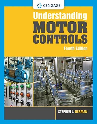 Understanding Motor ControlsMechanical EngineeringISBN:9781337798686Author:Stephen L. HermanPublisher:Delmar Cengage Learning
 Precision Machining Technology (MindTap Course Li...Mechanical EngineeringISBN:9781285444543Author:Peter J. Hoffman, Eric S. Hopewell, Brian JanesPublisher:Cengage Learning

Electrical Transformers and Rotating Machines
Mechanical Engineering
ISBN:9781305494817
Author:Stephen L. Herman
Publisher:Cengage Learning

Automotive Technology: A Systems Approach (MindTa...
Mechanical Engineering
ISBN:9781133612315
Author:Jack Erjavec, Rob Thompson
Publisher:Cengage Learning

Understanding Motor Controls
Mechanical Engineering
ISBN:9781337798686
Author:Stephen L. Herman
Publisher:Delmar Cengage Learning

Precision Machining Technology (MindTap Course Li...
Mechanical Engineering
ISBN:9781285444543
Author:Peter J. Hoffman, Eric S. Hopewell, Brian Janes
Publisher:Cengage Learning
Microelectronics Fabrication Center; Author: AnritsuCompany;https://www.youtube.com/watch?v=oDC6WWj3gmk;License: Standard Youtube License