
Videos
For the class−AB output stage in Figure 8.36, the parameters are:
(a)
The value of
Answer to Problem 8.49P
The value of the
Explanation of Solution
Calculation:
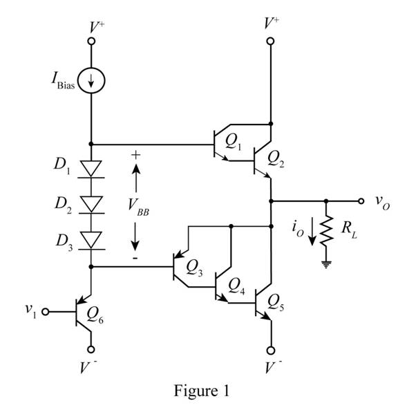
The given diagram is shown in Figure 1
The conversion from
The conversion from
The expression for the value of voltage
Substitute
The expression for the value of the voltage
The expression for the value of the voltage
The expression for the value of the voltage
The expression for the value of
The expression for the value of
The expression for the value of the voltage
Substitute
Substitute
Substitute
Substitute
Substitute
Substitute
Substitute
Substitute
Substitute
Conclusion:
Therefore, the value of the current
(b)
The value of the quiescent collector current in each transistor and the value of the collector quiescent current and the instantaneous power dissipated in
Answer to Problem 8.49P
The is
Explanation of Solution
Calculation:
The expression for the value of maximum output voltage is given by,
Substitute
The expression for the value of the current delivered to the load is given by,
Substitute
Apply KCL at the output node.
Substitute
The expression for the value of the current
Substitute
The expression for the value of the current
Substitute
The expression for the value of the voltage
Substitute
The expression for the value of the current
Substitute
The expression for the value of the current
Substitute
The expression for the value of power dissipated in the transistor
Substitute
The expression for the value of power dissipated in the transistor
Substitute
Conclusion:
Therefore, the value of the current
Want to see more full solutions like this?
Chapter 8 Solutions
Microelectronics: Circuit Analysis and Design


- Please solve this question step by step and handwritten and do not use chat gpt or ai tools thank you very much!arrow_forwardPlease solve question c and d step by step and handwritten and do not use chat gpt or ai tools thank you very much!arrow_forwardPlease solve questions d,e,f step by step and handwritten and do not use chat gpt or ai tools thank you very much!arrow_forward
- Please solve this question step by step and handwritten and do not use chat gpt or ai tools thank you very much!arrow_forwardPlease solve question c,d,e step by step and handwritten and do not use chat gpt or ai tools thank you very much!arrow_forwardQ1: Design a logic circuit for the finite-state machine described by the assigned table in Fig. 1: Using D flip-flops. a. b. Using T flip-flops. Present Next State Output State x=0 x=0 YE Y₁Y Y₁Y Z 00 00 01 0 0 от 00 0 0 10 00 10 11 00 10 0arrow_forward
 Introductory Circuit Analysis (13th Edition)Electrical EngineeringISBN:9780133923605Author:Robert L. BoylestadPublisher:PEARSON
 Delmar's Standard Textbook Of ElectricityElectrical EngineeringISBN:9781337900348Author:Stephen L. HermanPublisher:Cengage Learning
 Programmable Logic ControllersElectrical EngineeringISBN:9780073373843Author:Frank D. PetruzellaPublisher:McGraw-Hill Education
 Fundamentals of Electric CircuitsElectrical EngineeringISBN:9780078028229Author:Charles K Alexander, Matthew SadikuPublisher:McGraw-Hill Education
 Electric Circuits. (11th Edition)Electrical EngineeringISBN:9780134746968Author:James W. Nilsson, Susan RiedelPublisher:PEARSON
 Engineering ElectromagneticsElectrical EngineeringISBN:9780078028151Author:Hayt, William H. (william Hart), Jr, BUCK, John A.Publisher:Mcgraw-hill Education,