
Concept explainers
(a)
The maximum and the minimum value of the output voltage and the minimum corresponding input voltages for the circuit to operate in the linear region for given value of
(a)
Answer to Problem 8.20P
The maximum value of the output voltage is
Explanation of Solution
Calculation:
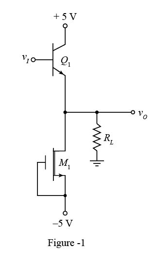
The given diagram is shown in Figure 1
The expression for the maximum value of the output voltage is given by,
Substitute
The expression for the drain to source saturation voltage is given by,
Substitute
The expression for the minimum value of the output voltage is given by,
Substitute
The expression for the minimum value of the input voltage is given by,
Substitute
The expression for the maximum value of the input voltage is given by,
Substitute
Conclusion:
Therefore, the maximum value of the output voltage is
(b)
The maximum and the minimum value of the output voltage and the minimum corresponding input voltages for the circuit to operate in the linear region for given value of
(b)
Answer to Problem 8.20P
The maximum value of the output voltage is
Explanation of Solution
Calculation:
The expression for the maximum value of the output voltage is given by,
Substitute
The expression for the drain to source saturation voltage is given by,
Substitute
The expression for the minimum value of the output voltage is given by,
Substitute
The expression for the minimum value of the input voltage is given by,
Substitute
The expression for the maximum value of the input voltage is given by,
Substitute
Conclusion:
Therefore, the maximum value of the output voltage is
(c)
The smallest value of the
(c)
Answer to Problem 8.20P
The minimum value of the load resistance is
Explanation of Solution
Calculation:
The expression for the current through the transistor
Substitute
The expression for the minimum value of the load resistance is
Substitute
The expression for the power delivered to the load is given by,
Substitute
The expression for the average power supplied by the source is given by,
Substitute
The expression for the value of power conversion efficiency is given by,
Substitute
Conclusion:
Therefore, the minimum value of the load resistance is
Want to see more full solutions like this?
Chapter 8 Solutions
Microelectronics: Circuit Analysis and Design


- A Three-phase, 12 pole, Y-connected alternator has 108 slots and 14 conductors per slot. The windings are (5/6 th) pitched. The flux per pole is 57 mWb distributed sinusoidally over the pole. If the machine runs at 500 r.p.m., determine the following: (a) The frequency of the generated e.m.f., (b) The distribution factor, (c) The pitch factor, and (d) The phase and line values of the generated e.m.f.?arrow_forwardTwo 3-ph, 6.6 kV, Y-connected, alternators supply a load of 3000 kW at 0.8 p.f. lagging. The synchronou impedance per phase of machine A is (0.5+110) and that of machine B is (0.4 +J12) . The excitation of machine A adjusted so that it delivers 150 A. The load is shared equally between the machines. Determine the armature curre p.f., induced e.m.f., and load angle of each machine?arrow_forwardName the circuit below? The output voltage is initially zero and the pulse width is 200 μs. Find the Vout and draw the output waveform? +2.5 V V 247 -2.5 V C 0.01 F Ri W 10 ΚΩarrow_forward
- Please work outarrow_forwardFind Vfinal when Vs up and Vs V. Which LED will light in each case? Red or Green? Justify your answers. Fill the table below. Vs 8 ΚΩ Vos Χρι + 3 ΚΩ www 6 ΚΩ ww 4 ΚΩ Yo www Vo Vec-12 V Nol V final Vm w 3 ΚΩ 5 V 38 ΚΩ R= 1 kQ V -12 V Red LED Green LED Vs Vo Vfinal Which LED is ON? Varrow_forwardCircuits help please solve and explain. Question in images providedarrow_forward
- + V 6.2 A 1.2 A S R 4 Ω Find the source voltage Vs 0.8 Aarrow_forwardDetermine i(t) for t≥ 0 given that the circuit below had been in steady state for a long time prior to t = 0. Also, I₁ = 1 5 A, R₁ =22, R2 =10 Q2, R3 = 32, R4 =7 2, and L=0.15 H. Also fill the table. m L ww R2 t = 0 R₁ 29 R3 R4 Time 0 iL(t) 0 8arrow_forwardPlease help explain this problemarrow_forward
- + P = 16 W w w P = 8 W I R₁ R2 E = RT=322 1- Determine R1, R2, E ΙΩarrow_forward+ 30 V = - 20 V + R 2- Use KVL to find the voltage V - V + + 8 Varrow_forwardFind the Thévenin equivalent circuit for the portions of the networks in Figure external to the elements between points a and b. a R₁ 2002 I = 0.1 A 0° Xc : 32 Ω R2 = 6802 20 Ω фъarrow_forward
 Introductory Circuit Analysis (13th Edition)Electrical EngineeringISBN:9780133923605Author:Robert L. BoylestadPublisher:PEARSON
 Delmar's Standard Textbook Of ElectricityElectrical EngineeringISBN:9781337900348Author:Stephen L. HermanPublisher:Cengage Learning
 Programmable Logic ControllersElectrical EngineeringISBN:9780073373843Author:Frank D. PetruzellaPublisher:McGraw-Hill Education
 Fundamentals of Electric CircuitsElectrical EngineeringISBN:9780078028229Author:Charles K Alexander, Matthew SadikuPublisher:McGraw-Hill Education
 Electric Circuits. (11th Edition)Electrical EngineeringISBN:9780134746968Author:James W. Nilsson, Susan RiedelPublisher:PEARSON
 Engineering ElectromagneticsElectrical EngineeringISBN:9780078028151Author:Hayt, William H. (william Hart), Jr, BUCK, John A.Publisher:Mcgraw-hill Education,