Loose Leaf for Engineering Circuit Analysis Format: Loose-leaf
9th Edition
ISBN: 9781259989452
Author: Hayt
Publisher: Mcgraw Hill Publishers
expand_more
expand_more
format_list_bulleted
Concept explainers
Videos
Textbook Question
Chapter 5, Problem 59E
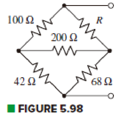
For the network of Fig. 5.98, select a value of R such that the network has an equivalent resistance of 70.6 Ω.
Expert Solution & Answer
Want to see the full answer?
Check out a sample textbook solution
Students have asked these similar questions
Crystallographic planes
Crystallographic planes are denoted by Miller indices.
5b
Algorithm for Miller indices
1. Read off intercepts of plane with axes in
terms of a, b, c
2. Take reciprocals of intercepts
3. Reduce to smallest integer values
4. Enclose in parentheses, no commas.
353
1/3 1/5 1/3
535
(535)
In the cubic system, a plane and a
direction with the same indices are
orthogonal. E.g. [100] direction is
perpendicular to (100) plane.
Correspondingly, [123] direction is
perpendicular to (123) plane.
[2,3,3]
Plane intercepts axes at 3a, 2b, 2c
2
11 1
Reciprocal numbers are:
3'2'2
b.
Indices of the plane (Miller): (2,3,3)
2
a
Indices of the direction: [2,3,3]
X
(200)
(100)
(110)
(111)
(100)
Indices of crystallographic plane can be found from cross product of indices of
any two non-parallel directions in this plane.
Crystallographic positions
Crystallographic position
is denoted by three
numbers, which are
coefficients of the
position vector, e.g. ½½½
for the red atom.
Here the 'new' atom is at a/2 + b/2 + c/2
Silicon crystal has so-called "diamond type lattice".
Each Si atom has 4 nearest neighbors.
Diamond lattice starts with a FCC lattice and then
adds four additional INTERNAL atoms at locations
r = a/4+b/4+c/4 away from each of the atoms. In
other words, diamond lattice is formed by two FCC
lattices sifted by the vector r.
find the answers for this prelab
Chapter 5 Solutions
Loose Leaf for Engineering Circuit Analysis Format: Loose-leaf
Ch. 5.1 - For the circuit of Fig. 5.4, use superposition to...Ch. 5.2 - For the circuit of Fig. 5.7, use superposition to...Ch. 5.2 - For the circuit of Fig. 5.18, compute the current...Ch. 5.2 - For the circuit of Fig. 5.20, compute the voltage...Ch. 5.3 - Using repeated source transformations, determine...Ch. 5.3 - Use Thvenins theorem to find the current through...Ch. 5.3 - Determine the Thvenin and Norton equivalents of...Ch. 5.3 - Find the Thvenin equivalent for the network of...Ch. 5.3 - Find the Thvenin equivalent for the network of...Ch. 5.4 - Consider the circuit of Fig. 5.43. FIGURE 5.43...
Ch. 5.5 - Prob. 11PCh. 5 - Linear systems are so easy to work with that...Ch. 5 - Prob. 2ECh. 5 - Prob. 3ECh. 5 - (a) Employ superposition to determine the current...Ch. 5 - (a) Using superposition to consider each source...Ch. 5 - (a) Determine the individual contributions of each...Ch. 5 - (a) Determine the individual contributions of each...Ch. 5 - After studying the circuit of Fig. 5.53, change...Ch. 5 - Consider the three circuits shown in Fig. 5.54....Ch. 5 - (a) Using superposition, determine the voltage...Ch. 5 - Employ superposition principles to obtain a value...Ch. 5 - (a) Employ superposition to determine the...Ch. 5 - Perform an appropriate source transformation on...Ch. 5 - (a) For the circuit of Fig. 5.59, plot iL versus...Ch. 5 - Determine the current labeled I in the circuit of...Ch. 5 - Verify that the power absorbed by the 7 resistor...Ch. 5 - (a) Determine the current labeled i in the circuit...Ch. 5 - (a) Using repeated source transformations, reduce...Ch. 5 - Prob. 19ECh. 5 - (a) Making use of repeated source transformations,...Ch. 5 - Prob. 21ECh. 5 - (a) With the assistance of source transformations,...Ch. 5 - For the circuit in Fig. 5.67 transform all...Ch. 5 - Prob. 24ECh. 5 - (a) Referring to Fig. 5.69, determine the Thevenin...Ch. 5 - (a) With respect to the circuit depicted in Fig....Ch. 5 - (a) Obtain the Norton equivalent of the network...Ch. 5 - (a) Determine the Thevenin equivalent of the...Ch. 5 - Referring to the circuit of Fig. 5.71: (a)...Ch. 5 - Prob. 30ECh. 5 - (a) Employ Thvenins theorem to obtain a...Ch. 5 - Prob. 32ECh. 5 - Determine the Norton equivalent of the circuit...Ch. 5 - For the circuit of Fig. 5.75: (a) Employ Nortons...Ch. 5 - (a) Obtain a value for the Thvenin equivalent...Ch. 5 - Prob. 36ECh. 5 - Obtain a value for the Thvenin equivalent...Ch. 5 - With regard to the network depicted in Fig. 5.79,...Ch. 5 - Determine the Thvenin and Norton equivalents of...Ch. 5 - Determine the Norton equivalent of the circuit...Ch. 5 - Prob. 41ECh. 5 - Determine the Thvenin and Norton equivalents of...Ch. 5 - Prob. 43ECh. 5 - Prob. 44ECh. 5 - Prob. 45ECh. 5 - (a) For the simple circuit of Fig. 5.87, find the...Ch. 5 - For the circuit drawn in Fig. 5.88, (a) determine...Ch. 5 - Study the circuit of Fig. 5.89. (a) Determine the...Ch. 5 - Prob. 49ECh. 5 - Prob. 50ECh. 5 - With reference to the circuit of Fig. 5.91, (a)...Ch. 5 - Prob. 52ECh. 5 - Select a value for RL in Fig. 5.93 such that it...Ch. 5 - Determine what value of resistance would absorb...Ch. 5 - Derive the equations required to convert from a...Ch. 5 - Convert the - (or "-") connected networks in Fig....Ch. 5 - Convert the Y-(or T-) connected networks in Fig....Ch. 5 - For the network of Fig. 5.97, select a value of R...Ch. 5 - For the network of Fig. 5.98, select a value of R...Ch. 5 - Prob. 60ECh. 5 - Calculate Rin as indicated in Fig.5.100. FIGURE...Ch. 5 - Employ Y conversion techniques as appropriate to...Ch. 5 - Prob. 63ECh. 5 - (a) Use appropriate techniques to obtain both the...Ch. 5 - (a) For the network in Fig. 5.104, replace the...Ch. 5 - Prob. 66ECh. 5 - Prob. 67ECh. 5 - A 2.57 load is connected between terminals a and...Ch. 5 - A load resistor is connected across the open...Ch. 5 - A backup is required for the circuit depicted in...Ch. 5 - (a) Explain in general terms how source...Ch. 5 - The load resistor in Fig. 5.108 can safely...Ch. 5 - Prob. 74ECh. 5 - As part of a security system, a very thin 100 ...Ch. 5 - With respect to the circuit in Fig. 5.90, (a)...
Knowledge Booster


Learn more about
Need a deep-dive on the concept behind this application? Look no further. Learn more about this topic, electrical-engineering and related others by exploring similar questions and additional content below.Similar questions
- Q2: (30 Marks) Design a DC/DC converter that produce output waveforms that shown in figures below from a fixed DC source of 20 volts. Vo (Volt) 14.1 IL (Amp) 13.9 2.25 1.75 † (msec) Output voltage 0.18 0.2 t (msec) L 0.214 0.22 Output currentarrow_forward6. Build the circuit shown in Figure 2 below in PSpice. Note that the power supply V1 is a VSIN power supply in the SOURCE library. Vcc is a VDC supply found in the SOURCE library. Model this circuit using the Time Domain (Transient) Analysis Type with a Run To Time of 2 ms. A. Paste your output graph showing the voltage at the base terminal, collector terminal and at the load. B. What is the voltage gain of the circuit? (Compare the voltage amplitude at the base terminal input (across Rb2) to that at the collector terminal. C. What happens to the output voltage at the collector terminal if the value of Rb1 is reduced by a factor of 10 (to 14.7 kn)? Simulate this situation and explain the result. D. What happens to the output voltage at the collector terminal if the value of Rb1 is increased by a factor of 3 (to 441 k)? Simulate this situation and explain the result. Rb1 RC 147k 1k C2 C1 Q1 Vcc 1u VOFF = 0 Q2N3904 10Vdc VAMPL = 0.1V1 1u FREQ = 2k R_load Rb2 Re AC = 0 250 40k 20 Figure…arrow_forwardThe input reactance of 1/2 dipole with radius of 1/30 is given as shown in figure below, Assuming the wire of dipole is conductor 5.6*107 S/m, determine at f=1 GHz the a-Loss resistance, b- Radiation efficiency c-Reflection efficiency when the antenna is connected to T.L shown in the figure. Rr Ro= 50 2 1/4 RL -j100 [In(l/a) - 1.5] tan(ẞl)arrow_forward
- 6) For each independent source in this circuit calculate the amount of power being supplied or the amount of power being absorbed + 6V www +3V- www 20 ми ми 352 0.5A + 3Varrow_forward2) A circuit is given as shown (a) Find and label circuit nodes. (b) Determine V, V₂, V₂, I₂ and I. + V₂ 452 m I2 6Ω www 52 t + V + 4A 노동 102 ww 1202 60 www I₂arrow_forwardA Darlington Pair consists of two transistors with the first BJT driving the base terminal of the second transistor as shown in the picture provided. What does the curve trace for a Darlington Pair of Bipolar Junction Transistors look like?arrow_forward
- Provide Pen and paper solution please not using AIarrow_forward5) If the current source supplies 448 watts, then what 15 the value of resistance R? ми R ↑ YA 62 ww 120 } ww 6_02 { wwarrow_forwardWhat is the equivalent resistance of this circuit between terminals A and B ? m 1852 A 7_A 122 도 www 50 ти B ww 36 Ω 201 www www 30√arrow_forward
- 3) A circuit is given as shown. (a) Find and label the circuit nodes. (6) Determine V2, V2, I₂, I₂ and Is © For each circuit element determine how much power it Supplies 15 absorbs. m 20 + 20 www 13 + 20 Z9V H 56 +1 LOV 1/2 1 4A + 3_22 3.2 ми + V₂ I 1arrow_forwardIn this experiment, we are going to use a 2N3904 BJT. Examine the data sheet for this device carefully. In particular, make a note of the current gain (identified by hFE). 1. Obtain the curve trace for a "Darlington Pair" of Bipolar Junction Transistors. A Darlington Pair consists of two transistors with the first BJT driving the base terminal of the second transistor as shown in Figure 1 below. A. Set up the primary sweep voltages for V1 the same as shown in the lecture notes (see the Darlington pair IV curve). B. Set up the secondary sweep currents for 11 to be an order of magnitude smaller than for the single BJT. In the Sweep Type box choose linear and enter the following 3 values: Start Value: 0, End Value: 8u and Increment: 1u (see lecture notes). C. Describe the primary differences you observe between the single BJT Curve Trace and that of the Darlington Pair. Discuss what might cause each difference. Q1 11 Q2 V1 Q2N3904 Figure 1. A Darlington Pair of 2N3904 transistors in a…arrow_forward2. Using the IV plots shown in Fig. 3 (and found in the reintroduction to PSpice) design a BJT biasing circuit that results in the following parameters: VCE = 2 Vand ig = 40 μA. We also require the power supply to be fixed at 5 Volts (this is where the load line intercepts the iB =ic = 0 line). You may use the circuit shown in Example 1. Note that all resistor values in Example 1 must be recalculated. Your solution for the base to ground and base to collector resistors may not be unique.arrow_forward
arrow_back_ios
SEE MORE QUESTIONS
arrow_forward_ios
Recommended textbooks for you
 Delmar's Standard Textbook Of ElectricityElectrical EngineeringISBN:9781337900348Author:Stephen L. HermanPublisher:Cengage Learning
Delmar's Standard Textbook Of Electricity
Electrical Engineering
ISBN:9781337900348
Author:Stephen L. Herman
Publisher:Cengage Learning
Z Parameters - Impedance Parameters; Author: Electrical Engineering Authority;https://www.youtube.com/watch?v=qoD4AoNmySA;License: Standard Youtube License