Microelectronics: Circuit Analysis and Design
4th Edition
ISBN: 9780073380643
Author: Donald A. Neamen
Publisher: McGraw-Hill Companies, The
bartleby

Concept explainers

bartleby

Videos

Textbook Question
Book Icon
Chapter 10, Problem 10.6TYU

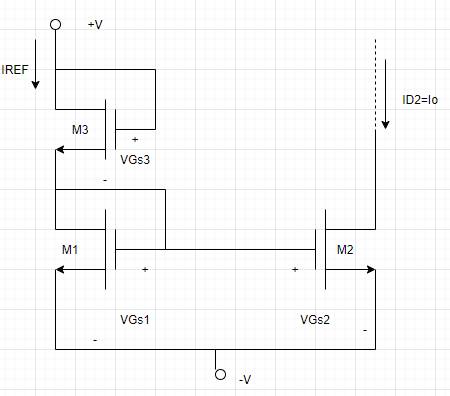
The bias voltages of the MOSFET current source in Figure 10.17 are V + = 3 V and V = 3 V . The transistor parameters are V T N = 0.5 V , k n = 80 μ A / V 2 , and λ = 0.02 V 1 . The transistor width-to-length ratios are ( W / L ) 3 = 3 , ( W / L ) 1 = 12 , and ( W / L ) 2 = 6 . Determine: (a) I R E F , (b) I O at V D S 2 = 2 V , and (e) I O at V D S 2 = 4 V . (Ans. (a) I R E F = 1.33 m A , (b) I O = 0.6936 m A , (c) I O = 0.7203 m A )

(a)

Expert Solution
Check Mark
To determine

The reference current IREF .

Answer to Problem 10.6TYU

  IREF=1.39mA

Explanation of Solution

Given Information:

  V+=3VV=3V

    VTN=0.5VK'n=80μA/V2λ=0.02V1 (W/L) 1 =12 (W/L) 2 =6 (W/L) 3 =3

Calculation:

  Microelectronics: Circuit Analysis and Design, Chapter 10, Problem 10.6TYU , additional homework tip  1

According to the circuit the reference current will be,

  IREF=K'n2(WL)1(VGS1VTN1)2(1+λVDS1)

Substitute given values in above expression,

     I REF = 80× 10 6 2 ( 12 ) ( V GS1 0.5) 2 (1+(0.02) V DS1 )   I REF =480× 10 6 ( V GS1 0.5) 2 [ 1+(0.02) V DS1 ]( 1 )

The gate- to- source voltage VGS1 will be,

  VGS1= ( W/L ) 3 ( W/L ) 1 1+ ( W/L ) 3 ( W/L ) 1 (V+V)+1 ( W/L ) 3 ( W/L ) 1 1+ ( W/L ) 3 ( W/L ) 1 VTN

Substitute given values in above expression,

  VGS1=3 121+3 12(3(3)+13 121+3 12(0.5)

  VGS1=0.51.5(6)+0.51.5(0.5)VGS1=2+0.167VGS1=2.167V

As VDS1=VGS1=2.167V so substitute the values in equation (1),

   I REF =480× 10 6 (2.1670.5) 2 [ 1+(0.02)(2.167) ]IREF=1.39mA

(b)

Expert Solution
Check Mark
To determine

The load current IO for the given value of VDS2 .

Answer to Problem 10.6TYU

  IO=0.6936mA

Explanation of Solution

Given Information:

  V+=3VV=3V

    VTN=0.5VK'n=80μA/V2λ=0.02V1 (W/L) 1 =12 (W/L) 2 =6 (W/L) 3 =3

  VDS2=2V

Calculation:

  Microelectronics: Circuit Analysis and Design, Chapter 10, Problem 10.6TYU , additional homework tip  2

According to the circuit the reference current will be,

  IREF=K'n2(WL)1(VGS1VTN1)2(1+λVDS1)

Substitute given values in above expression,

     I REF = 80× 10 6 2 ( 12 ) ( V GS1 0.5) 2 (1+(0.02) V DS1 )   I REF =480× 10 6 ( V GS1 0.5) 2 [ 1+(0.02) V DS1 ]( 1 )

The gate- to- source voltage VGS1 will be,

  VGS1= ( W/L ) 3 ( W/L ) 1 1+ ( W/L ) 3 ( W/L ) 1 (V+V)+1 ( W/L ) 3 ( W/L ) 1 1+ ( W/L ) 3 ( W/L ) 1 VTN

Substitute given values in above expression,

  VGS1=3 121+3 12(3(3)+13 121+3 12(0.5)

  VGS1=0.51.5(6)+0.51.5(0.5)VGS1=2+0.167VGS1=2.167V

As VDS1=VGS1=2.167V so substitute the values in equation (1),

   I REF =480× 10 6 (2.1670.5) 2 [ 1+(0.02)(2.167) ]IREF=1.39mA

Now calculate load current IO for VDS2=2V ,

  IO=(W/L)2(W/L)1(1+λV DS21+λV DS1)IREF

Substitute given values in above expression

  IO=612( 1+(0.02)(2) 1+(0.02)(2.167))(1.39×10³)IO=0.6936mA

(c)

Expert Solution
Check Mark
To determine

The load current IO for given value of VDS2 .

Answer to Problem 10.6TYU

  IO=0.72mA

Explanation of Solution

Given Information:

  V+=3VV=3V

    VTN=0.5VK'n=80μA/V2λ=0.02V1 (W/L) 1 =12 (W/L) 2 =6 (W/L) 3 =3

  VDS2=4V

Calculation:

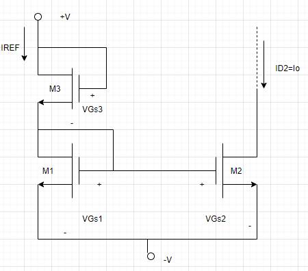
Consider the given circuit.
  Microelectronics: Circuit Analysis and Design, Chapter 10, Problem 10.6TYU , additional homework tip  3

According to the circuit the reference current will be,

  IREF=K'n2(WL)1(VGS1VTN1)2(1+λVDS1)

Substitute given values in above expression,

     I REF = 80× 10 6 2 ( 12 ) ( V GS1 0.5) 2 (1+(0.02) V DS1 )   I REF =480× 10 6 ( V GS1 0.5) 2 [ 1+(0.02) V DS1 ]( 1 )

The gate- to- source voltage VGS1 will be,

  VGS1= ( W/L ) 3 ( W/L ) 1 1+ ( W/L ) 3 ( W/L ) 1 (V+V)+1 ( W/L ) 3 ( W/L ) 1 1+ ( W/L ) 3 ( W/L ) 1 VTN

Substitute given values in above expression,

  VGS1=3 121+3 12(3(3)+13 121+3 12(0.5)

  VGS1=0.51.5(6)+0.51.5(0.5)VGS1=2+0.167VGS1=2.167V

As VDS1=VGS1=2.167V so substitute the values in equation (1),

   I REF =480× 10 6 (2.1670.5) 2 [ 1+(0.02)(2.167) ]IREF=1.39mA

Now calculate load current IO for VDS2=4V ,

  IO=(W/L)2(W/L)1(1+λV DS21+λV DS1)IREF

Substitute given values in above expression

  IO=612( 1+(0.02)(4) 1+(0.02)(2.167))(1.39×10³)IO=0.72mA

Want to see more full solutions like this?

Subscribe now to access step-by-step solutions to millions of textbook problems written by subject matter experts!
Students have asked these similar questions
Solve by pen & paper without using chatgpt or AI Mesh analysis
Solve by hand do not use chatgpt or AI otherwise downvote
Don't use ai to answer I will report you answer

Chapter 10 Solutions

Microelectronics: Circuit Analysis and Design

Ch. 10 - Prob. 10.4TYUCh. 10 - Prob. 10.8EPCh. 10 - Prob. 10.9EPCh. 10 - Consider the JFET circuit in Figure 10.24. The...Ch. 10 - Consider Design Example 10.8. Assume transistor...Ch. 10 - The bias voltages of the MOSFET current source in...Ch. 10 - Prob. 10.7TYUCh. 10 - All transistors in the MOSFET modified Wilson...Ch. 10 - A simple BJT amplifier with active load is shown...Ch. 10 - Prob. 10.9TYUCh. 10 - Prob. 10.10TYUCh. 10 - Prob. 10.11TYUCh. 10 - Prob. 10.12EPCh. 10 - For the circuit in Figure 10.40(a), the transistor...Ch. 10 - Prob. 10.12TYUCh. 10 - Repeat Example 10.12 for the case where a resistor...Ch. 10 - Prob. 10.14TYUCh. 10 - Prob. 1RQCh. 10 - Explain the significance of the output resistance...Ch. 10 - Prob. 3RQCh. 10 - Prob. 4RQCh. 10 - What is the primary advantage of a BJT cascode...Ch. 10 - Prob. 6RQCh. 10 - Can a piecewise linear model of the transistor be...Ch. 10 - Prob. 8RQCh. 10 - Sketch the basic MOSFET two-transistor current...Ch. 10 - Discuss the effect of mismatched transistors on...Ch. 10 - Prob. 11RQCh. 10 - Sketch a MOSFET cascode current source circuit and...Ch. 10 - Discuss the operation of an active load.Ch. 10 - What is the primary advantage of using an active...Ch. 10 - Prob. 15RQCh. 10 - What is the impedance seen looking into a simple...Ch. 10 - What is the advantage of using a cascode active...Ch. 10 - Prob. 10.1PCh. 10 - The matched transistors Q1 and Q2 in Figure...Ch. 10 - Prob. 10.3PCh. 10 - Reconsider the circuit in Figure 10.2(a). Let...Ch. 10 - Prob. 10.5PCh. 10 - The transistor and circuit parameters for the...Ch. 10 - The bias voltages in the circuit shown in Figure...Ch. 10 - Consider the current source in Figure 10.2(b). The...Ch. 10 - Prob. 10.9PCh. 10 - Prob. 10.10PCh. 10 - Prob. D10.11PCh. 10 - In the circuit in Figure P10.11, the transistor...Ch. 10 - Prob. D10.13PCh. 10 - Consider the circuit shown in Figure P 10.14. The...Ch. 10 - Design a basic two-transistor current...Ch. 10 - The values of for the transistors in Figure P10.16...Ch. 10 - Consider the circuit in Figure P10.17. The...Ch. 10 - All transistors in the N output current mirror in...Ch. 10 - Design a pnp version of the basic three-transistor...Ch. 10 - Prob. D10.20PCh. 10 - Consider the Wilson current source in Figure...Ch. 10 - Consider the circuit in Figure P10.22. The...Ch. 10 - Consider the Wilson current-source circuit shown...Ch. 10 - Consider the Widlar current source shown in Figure...Ch. 10 - Prob. 10.25PCh. 10 - Consider the circuit in Figure P10.26. Neglect...Ch. 10 - (a) For the Widlar current source shown in Figure...Ch. 10 - Consider the Widlar current source in Problem...Ch. 10 - (a) Design the Widlar current source such that...Ch. 10 - Design a Widlar current source to provide a bias...Ch. 10 - Design the Widlar current source shown in Figure...Ch. 10 - The circuit parameters of the Widlar current...Ch. 10 - Consider the Widlar current source in Figure 10.9....Ch. 10 - Consider the circuit in Figure P10.34. The...Ch. 10 - The modified Widlar current-source circuit shown...Ch. 10 - Consider the circuit in Figure P10.36. Neglect...Ch. 10 - Consider the Widlar current-source circuit with...Ch. 10 - Assume that all transistors in the circuit in...Ch. 10 - In the circuit in Figure P10.39, the transistor...Ch. 10 - Consider the circuit in Figure P10.39, with...Ch. 10 - Consider the circuit shown in Figure P10.41....Ch. 10 - For the circuit shown in Figure P 10.42, assume...Ch. 10 - Consider the circuit in Figure P10.43. The...Ch. 10 - Consider the MOSFET current-source circuit in...Ch. 10 - The MOSFET current-source circuit in Figure P10.44...Ch. 10 - Consider the basic two-transistor NMOS current...Ch. 10 - Prob. 10.47PCh. 10 - Consider the circuit shown in Figure P10.48. Let...Ch. 10 - Prob. 10.49PCh. 10 - The circuit parameters for the circuit shown in...Ch. 10 - Prob. 10.51PCh. 10 - Figure P10.52 is a PMOS version of the...Ch. 10 - The circuit shown in Figure P10.52 is biased at...Ch. 10 - The transistor circuit shown in Figure P10.54 is...Ch. 10 - Assume the circuit shown in Figure P10.54 is...Ch. 10 - The circuit in Figure P 10.56 is a PMOS version of...Ch. 10 - The transistors in Figure P10.56 have the same...Ch. 10 - Consider the NMOS cascode current source in Figure...Ch. 10 - Consider the NMOS current source in Figure P10.59....Ch. 10 - Prob. 10.60PCh. 10 - The transistors in the circuit shown in Figure...Ch. 10 - A Wilson current mirror is shown in Figure...Ch. 10 - Repeat Problem 10.62 for the modified Wilson...Ch. 10 - Prob. 10.64PCh. 10 - Prob. 10.65PCh. 10 - Prob. D10.66PCh. 10 - Prob. D10.67PCh. 10 - The parameters of the transistors in the circuit...Ch. 10 - Prob. 10.69PCh. 10 - Consider the circuit shown in Figure P10.70. The...Ch. 10 - Prob. 10.71PCh. 10 - Prob. D10.72PCh. 10 - Prob. 10.73PCh. 10 - Prob. D10.74PCh. 10 - Prob. 10.75PCh. 10 - For the circuit shown in Figure P10.76, the...Ch. 10 - Prob. 10.77PCh. 10 - Prob. 10.78PCh. 10 - The bias voltage of the MOSFET amplifier with...Ch. 10 - Prob. 10.80PCh. 10 - Prob. 10.81PCh. 10 - Prob. 10.82PCh. 10 - A BJT amplifier with active load is shown in...Ch. 10 - Prob. 10.84PCh. 10 - Prob. 10.85PCh. 10 - Prob. 10.86PCh. 10 - The parameters of the transistors in Figure P10.87...Ch. 10 - The parameters of the transistors in Figure P10.88...Ch. 10 - A BJT cascode amplifier with a cascode active load...Ch. 10 - Design a bipolar cascode amplifier with a cascode...Ch. 10 - Design a MOSFET cascode amplifier with a cascode...Ch. 10 - Design a generalized Widlar current source (Figure...Ch. 10 - The current source to be designed has the general...Ch. 10 - Designa PMOS version of the current source circuit...Ch. 10 - Consider Exercise TYU 10.10. Redesign the circuit...
Knowledge Booster
Background pattern image
Electrical Engineering
Learn more about
Need a deep-dive on the concept behind this application? Look no further. Learn more about this topic, electrical-engineering and related others by exploring similar questions and additional content below.
Similar questions
SEE MORE QUESTIONS
Recommended textbooks for you
Text book image
Introductory Circuit Analysis (13th Edition)
Electrical Engineering
ISBN:9780133923605
Author:Robert L. Boylestad
Publisher:PEARSON
Text book image
Delmar's Standard Textbook Of Electricity
Electrical Engineering
ISBN:9781337900348
Author:Stephen L. Herman
Publisher:Cengage Learning
Text book image
Programmable Logic Controllers
Electrical Engineering
ISBN:9780073373843
Author:Frank D. Petruzella
Publisher:McGraw-Hill Education
Text book image
Fundamentals of Electric Circuits
Electrical Engineering
ISBN:9780078028229
Author:Charles K Alexander, Matthew Sadiku
Publisher:McGraw-Hill Education
Text book image
Electric Circuits. (11th Edition)
Electrical Engineering
ISBN:9780134746968
Author:James W. Nilsson, Susan Riedel
Publisher:PEARSON
Text book image
Engineering Electromagnetics
Electrical Engineering
ISBN:9780078028151
Author:Hayt, William H. (william Hart), Jr, BUCK, John A.
Publisher:Mcgraw-hill Education,
Optical fiber cables, how do they work? | ICT #3; Author: Lesics;https://www.youtube.com/watch?v=jZOg39v73c4;License: Standard Youtube License