
Videos
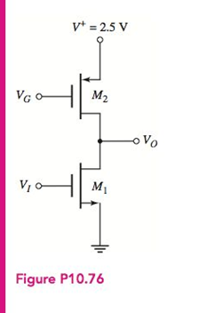
For the circuit shown in Figure P10.76, the transistor parameters are
(a)
The
Answer to Problem 10.76P
Explanation of Solution
Given:
Calculation:
The given circuit is,

The small-signal voltage gain is given, the expression for gain is,
Substituting the given values,
Substitute
Now substitute the given values in above expression,
It is known that,
On putting the given values,
Now substitute the value of
The drain current
Hence
Substitute
Put the value of
Conclusion:
(b)
The voltage
Answer to Problem 10.76P
Explanation of Solution
Given:
Calculation:
The given circuit is,

The small-signal voltage gain is given, the expression for gain is,
Substituting the given values,
Substitute
Now substitute the given values in above expression,
It is known that,
On putting the given values,
Now substitute the value of
The drain current
Hence
Substitute
Put the value of
Substitute
Conclusion:
(c)
The voltage
Answer to Problem 10.76P
Explanation of Solution
Given:
Calculation:
The given circuit is,
The small-signal voltage gain is given, the expression for gain is,
Substituting the given values,
Substitute
Now substitute the given values in above expression,
It is known that,
On putting the given values,
Now substitute the value of
The drain current
Hence
Substitute
Put the value of
Since
The drain current
On substituting the given values,
Now the gate voltage will be,
Conclusion:
Want to see more full solutions like this?
Chapter 10 Solutions
Microelectronics: Circuit Analysis and Design


- 2) In the ideal transformer circuit shown below find Vo and the complex power supplied by the source. 292 www b 1:4 16 Ω ww + + 240/0° V rms -12492arrow_forward3) In the ideal autotransformer circuit shown below find 11, 12 and lo. Find the average power delivered to the load. (hint: write KVL for both sides) 20/30° V(+ 2-1602 200 turns V₂ 10 + j40 Ω 80 turns V₁arrow_forward1) Find Vo in the following circuit. Assume the mesh currents are clockwise. ΠΩ Ω ΖΩ ww 1Ω ww 24/0° (± 6 Ω j4 Ω 1Ω +arrow_forward
- Please show all stepsarrow_forward11-3) similar to Lathi & Ding, Prob. P.6.8-1 Consider the carrier modulator shown in the figure below, which transmits a binary carrier signal. The baseband generator uses polar NRZ signaling with rectangular pulses. The data rate is 8 Mbit/s. (a) If the modulator generates a binary PSK signal, what is the bandwidth of the modulated output? (b) If the modulator generates FSK with the difference fel - fco = 6 MHz (cf. Fig 6.32c), determine the modulated signal bandwidth. Binary data source Baseband signal generator Modulated output Modulator N-E---arrow_forwardSolve this problem and show all of the workarrow_forward
- Q3: Why is the DRAM cell design simpler but slower than SRAM?arrow_forward5052 ми a JXL 000 +2 16s (wt) bi jxc M 100♫ ZL. Find the Value of XL & X c if the Circuit trans for Max. Power to (ZL).arrow_forwardChoose the best answer for each: 1. What does SRAM use to store data? 。 a) Capacitors ob) Latches 。 c) Flip-flops od) Transistors 2. Which RAM type requires refreshing? o a) SRAM ob) DRAM 。 c) ROM od) Flash 3. What type of memory retains data only while power is on? a) ROM 。 b) EEPROM o c) DRAM od) Flash 4. How many addresses can a 15-bit address bus handle? o a) 32k • b) 64k o c) 16k od) lk 5. What operation occurs when data is copied out of memory without erasing? oa) Write ob) Read o c) Refresh o d) Load 6. DRAM cells store bits using: a) Flip-flops 。 b) Capacitors c) Diodes od) Resistors 7. The cache located inside the CPU is: 。 a) L2 cache o b) LI cache °c) ROM od) HDD 8. SDRAM is synchronized with: o a) Cache ob) Data Bus c) System Clock od) Hard Disk 9. The bus that carries commands is called: o a) Data Bus b) Control Bus o c) Address Bus o d) Logic Bus 10. What is the main use of SRAM? o Disk storage o Cache o Main memory o Registers 11. The smallest addressable unit in…arrow_forward
- Q4: A cache memory is 128k × 16. How many bytes can it store?arrow_forwardSketch the output of the analogue computer shown below and find its closest describing function [suppose any variable to find the DF] +1 ew2 HI e2 1.0 +21 LO SJ eo SJ ew LO 1.0 +|e1| HI -1 ew1 ek(1 + e。) |e1| k = 1+|e1| Figure V-5 Feedback Limiter Behavior ROUNDED, DUE TO DIODE NONLINEARITY LIMIT VOLTAGE 409 DIODE CONDUCTS First, write the output transaction, then draw the output wave, and then find the Describing function. I need to solve the question step by step, with an explanation of each step.arrow_forwardSketch the output of the analogue computer shown below and find its closest describing function [suppose any variable to find the DF] SJ ew2 ew₁ HI |e2| 2 LO 1.0 +21 LO -1 HI Jel 1.0+|e1| ROUNDED, DUE TO DODE NONLINEARITY LIMIT VOLTAGE DIODE CONDUCTS ew1e, -k(1+ e。) k = |e1| 1+|e1| Figure 1-5 Feedback Limiter Behavior First, write the output transaction, then draw the output wave, and then find the Describing function. I need to solve the question step by step, with an explanation of each step.arrow_forward
 Introductory Circuit Analysis (13th Edition)Electrical EngineeringISBN:9780133923605Author:Robert L. BoylestadPublisher:PEARSON
 Delmar's Standard Textbook Of ElectricityElectrical EngineeringISBN:9781337900348Author:Stephen L. HermanPublisher:Cengage Learning
 Programmable Logic ControllersElectrical EngineeringISBN:9780073373843Author:Frank D. PetruzellaPublisher:McGraw-Hill Education
 Fundamentals of Electric CircuitsElectrical EngineeringISBN:9780078028229Author:Charles K Alexander, Matthew SadikuPublisher:McGraw-Hill Education
 Electric Circuits. (11th Edition)Electrical EngineeringISBN:9780134746968Author:James W. Nilsson, Susan RiedelPublisher:PEARSON
 Engineering ElectromagneticsElectrical EngineeringISBN:9780078028151Author:Hayt, William H. (william Hart), Jr, BUCK, John A.Publisher:Mcgraw-hill Education,