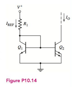
Consider the circuit shown in Figure P 10.14. The transistor Q 2 is equivalentto two identical transistors in parallel, each of which is matched to Q 1 . Assume the transistor parameters are V B E ( o n ) = 0.7 V , β = 60 , and V A = ∞ ,and assume the bias voltage is V + = 2.5 V . Design the circuit such that I O = 0.50 m A and determine the value of I R E F .
Consider the circuit shown in Figure P 10.14. The transistor Q 2 is equivalentto two identical transistors in parallel, each of which is matched to Q 1 . Assume the transistor parameters are V B E ( o n ) = 0.7 V , β = 60 , and V A = ∞ ,and assume the bias voltage is V + = 2.5 V . Design the circuit such that I O = 0.50 m A and determine the value of I R E F .
Solution Summary: The author calculates that transistor Q_2 is equivalent to two identical transistors in parallel.
Consider the circuit shown in Figure P 10.14. The transistor
Q
2
is equivalentto two identical transistors in parallel, each of which is matched to
Q
1
. Assume the transistor parameters are
V
B
E
(
o
n
)
=
0.7
V
,
β
=
60
, and
V
A
=
∞
,and assume the bias voltage is
V
+
=
2.5
V
. Design the circuit such that
I
O
=
0.50
m
A
and determine the value of
I
R
E
F
.
Design a counter to count-up from 2 to 7 using three of
D Flip Flops
(3) 3-Bit Count up (3 to 5) Using D Flip-Flop:
The State Equation of D Flip-Flop:
Q(t+1)=D(t) => Dn=Qn
Present State
D Flip-Flop
Next State
n
Q2p Q1p Q0p
3
0 1
1
1
Q2n Q1n Q0n D2 D1 D0
0 0 1 0 0
4
1
0
0
1
0
1
1 0
1
5
1 0
1
0
1
1
01
1
D2-Sum(3,4) and don't care X-Sum(0,1,2,6,7)
D1=Sum(5) and don't care X=Sum(0,1,2,6,7)
D0=Sum(4,5) and don't care X=Sum(0,1,2,6,7)
Using K-map to simplify the functions:
D2=Q1+Q0'
D1=Q1'QO
DO=Q1'
XOX
XOX
Q2 10
Q2 01
Q2 1xx
Q0
QO
Qo
D2 Q2
>CK
Q2
D1 Q1
BCD
CK
Q1
DO QF
►CK
Q0
☐ Present State Next State D Flip-Flop
n Q2p Q1p Q0p Q2n Q1n Q0n D2 D1 D0
2 0 1
0
0 1 1 0 1 1
3 0
1
1
1
0
0 1 00
4
1
0
0
1
0
1
1
0
1
5
1
0
1
1
1
0
1 1
0
6
1
1
0
0
1
0
0
1
0
D2
D2=Sum(3,4,5), X=Sum(0,1,7)
D1
Q2
1
Q1
1
0
☑
0
Qo
D2=Q0+Q1'
✗
0
Q1
Consider the following 4×1 multiplexer with inputs:
w0=2, w1=1, w2=x2' and w3=0
And with switches:
S1 x1 and S0=x0
What is the multiplexer output f as a function of x2, x1
and x0?
I need help adding a capacitor and a Zener diode to my circuit. I’m looking for a simple sketch or diagram showing how to connect them. i want diagram with final circuit after adding the zener diad and capacitor. don't do calclution or anything. thanks
Need a deep-dive on the concept behind this application? Look no further. Learn more about this topic, electrical-engineering and related others by exploring similar questions and additional content below.


 Introductory Circuit Analysis (13th Edition)Electrical EngineeringISBN:9780133923605Author:Robert L. BoylestadPublisher:PEARSON
 Delmar's Standard Textbook Of ElectricityElectrical EngineeringISBN:9781337900348Author:Stephen L. HermanPublisher:Cengage Learning
 Programmable Logic ControllersElectrical EngineeringISBN:9780073373843Author:Frank D. PetruzellaPublisher:McGraw-Hill Education
 Fundamentals of Electric CircuitsElectrical EngineeringISBN:9780078028229Author:Charles K Alexander, Matthew SadikuPublisher:McGraw-Hill Education
 Electric Circuits. (11th Edition)Electrical EngineeringISBN:9780134746968Author:James W. Nilsson, Susan RiedelPublisher:PEARSON
 Engineering ElectromagneticsElectrical EngineeringISBN:9780078028151Author:Hayt, William H. (william Hart), Jr, BUCK, John A.Publisher:Mcgraw-hill Education,