
Videos
Consider the circuit shown in Figure P6.19 where the signal−source is
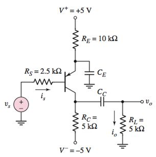
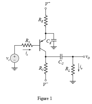
Figure P6.19
(a)
The small signal voltage gain
Answer to Problem 6.19P
The small signal voltage gain
Explanation of Solution
Given:
The sinusoidal source voltage
The circuit for
The current gain
The circuit parameters are shown below.
Concept used:
The expression for small signal voltage gain
The expression for transconductance is written below.
Calculation:
Apply dc analysis and KVL in base emitter
Substitute
The quiescent collector current is calculated as,
The transconductance is calculated as,
The diffusion resistance is calculated as,
Substitute
Therefore, the small signal voltage gain
The output current
Substitute
Therefore, the transconductance function
The output current is calculated as,
Therefore, the output current
The output voltage is calculated as,
Substitute
Therefore, the output voltage
Conclusion:
Thus, the small signal voltage gain
(b)
The small signal voltage gain
Answer to Problem 6.19P
The small signal voltage gain
Explanation of Solution
Given:
The current gain
Calculation:
Apply dc analysis and KVL in base emitter
Substitute
The quiescent collector current is calculated as,
The transconductance is calculated as,
The diffusion resistance is calculated as,
Substitute
Therefore, the small signal voltage gain
The output current
Substitute
Therefore, the transconductance function
The output current is calculated as,
Therefore, the output current
The output voltage is calculated as,
Substitute
Therefore, the output voltage
Conclusion:
Thus, the small signal voltage gain
Want to see more full solutions like this?
Chapter 6 Solutions
Microelectronics: Circuit Analysis and Design


- = Calculate Avf, Zif, and Zof for the amplifier circuit,Assume he = 50, hie 1.1k2, and identical transistors? 150kQ Vs 5002 HH +25v 10k +6 · 47ΚΩ 47k2 4.7k0} 33 ΚΩ 4.7ΚΩ 10k w 4.7kQ HH Voarrow_forwardFor the four-pole filter in Fig. (2), determine the capacitance values required to produce a critical frequency of 2680 Hz if all the resistors in the RC low-pass circuits are 1.8 K. Also select values for the feedback resistors to get a Butterworth response. Note: For a Butterworth response, the damping factor must be 1.848 for the first stage and 0.765 for the second stage. (2) Re Res ww " = 11arrow_forwardFor the circuit shown in Fig. 2.20, the transistors are identica' and have the following parameters: hje=50, hie = 1.1K, hr =0, and hoe = 0. Calculate Auf, Rif and Rof. Ans: 45.4; 112 KN; 129N. HH 150k 47k R 25 V 10k 47k 4.7k 5μF 33k 4.7k 50µF 50µF 4.7k 4.7k R₁ Roj R1000arrow_forward
- A triangular wave is applied to the input of Fig. (3). Determine what the output should be and sketch its waveform in relation to the input. 10μs. 0 5μs 15 μs 0.001 μF R₁ w 2.2karrow_forwardA three-phase, 480-V, 60-Hz, 6-pole, Y-connected induction motor has its speed controlled by slip power. The circuit parameters are given: Rs=0.06 ohms, Rr=0.05 ohms, Xs=0.2 ohms, Xr=0.3 ohms and Xm=6 ohms. The turn ratio of the rotor to stator winding is n=0.8. The no-load losses of the motor are equal to 150 W. The rotor and stator cupper losses are equal to 249.21 W. The slip power losses are estimated to 8000W. The load torque is 173.61 N.m. at 700 rpm. The efficiency is equal to: Select one: a. 71.5% b. None of these c. 81.5% d. 91.5% Question 2 Consider a 3-phase, 460-V, 100-hp, 0.88 power factor lagging, 4-pole, 1728 RPM, 60 Hz, Y-connected induction motor. The operating slip is equal to: Select one: a. 0.05 b. 0.01 c. 0.04 d. None of these Question 3 A 3 phase, 10 kW, 1750 rpm, Y- connected 460 V, 60 Hz, 4 poles, Y-connected induction motor has the following parameters: Rs = 0.5 Ohms, Rr = 0.3 Ohms, Xs = 0.9 Ohms, Xr = 0.9 Ohms, Xm = 25 Ohms. The no load…arrow_forwardelectric plants do for hand writingarrow_forward
- A lighting load of 600 kW and a motor load of 707 kW at 0.707 p.f lagging are supplied by two alternators running in parallel. One machine supplies 900 kW at 0.9 p.f lagging. Find the load sharing and p.f of second machine?arrow_forwardPlease draw out the circuitsarrow_forwardQ2 but when you get to part 3, can you please draw it outarrow_forward
- please solve manually. I need the drawing and the values too. Thank you!arrow_forwardTwo alternators, Y-connected 6.6 kV supply a load of 3000 kW at 0.8 p.f lagging. The synchronous mpedance of first alternator is (0.5+j10) Q/ph and second alternator is (0.4+j12) /ph. First alternator delivers 150 amp at 0.875 lag p.f. The two alterators are shared load equally. Determine the current, p.f., induced e.m.f, load angel, and maximum developed power of each alternator?arrow_forwardA domestic load of 2300 kW at 0.88 p.f lagging and a motors load of 3400 kW at 0.85 p.f lagging are supplied by two alternators operating in parallel. If one alternator is delivering a load of 3300 kW at 0.9 p.f lagging, what will be the output power and p.f of the other alternator?arrow_forward
 Introductory Circuit Analysis (13th Edition)Electrical EngineeringISBN:9780133923605Author:Robert L. BoylestadPublisher:PEARSON
 Delmar's Standard Textbook Of ElectricityElectrical EngineeringISBN:9781337900348Author:Stephen L. HermanPublisher:Cengage Learning
 Programmable Logic ControllersElectrical EngineeringISBN:9780073373843Author:Frank D. PetruzellaPublisher:McGraw-Hill Education
 Fundamentals of Electric CircuitsElectrical EngineeringISBN:9780078028229Author:Charles K Alexander, Matthew SadikuPublisher:McGraw-Hill Education
 Electric Circuits. (11th Edition)Electrical EngineeringISBN:9780134746968Author:James W. Nilsson, Susan RiedelPublisher:PEARSON
 Engineering ElectromagneticsElectrical EngineeringISBN:9780078028151Author:Hayt, William H. (william Hart), Jr, BUCK, John A.Publisher:Mcgraw-hill Education,