
Videos
For the transistor in the circuit in Figure P6.26, the parameters are
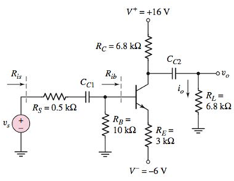
Figure P6.26
(a)
The quiescent
Answer to Problem 6.26P
The quiescent
Explanation of Solution
Given:
The current gain
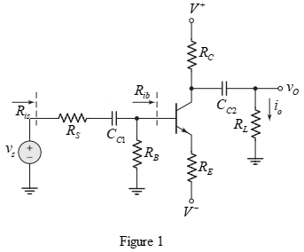
The circuit for
The circuit parameters are written below.
Concept used:
The expression for quiescent collector current is written below.
Calculation:
Apply dc analysis and KVL in base emitter loop.
Substitute
Substitute
Therefore, the quiescent collector current
Apply KVL in base collector loop.
Substitute
Therefore, the
Conclusion:
Thus, the quiescent
(b)
The hybrid
Answer to Problem 6.26P
The transconductance
Explanation of Solution
Concept used:
The expression for transconductance
The expression for diffusion resistance
The expression for output resistance
Calculation:
Substitute
Therefore, the transconductance
Substitute
Therefore, the diffusion resistance
Substitute
Therefore, the output resistance
Conclusion:
Thus, the transconductance
(c)
The small signal voltage gain
Answer to Problem 6.26P
The small signal voltage gain
Explanation of Solution
Concept used:
The expression for small signal voltage gain
The expression for small signal current gain
Calculation:
The input resistance
Substitute
Therefore, the small signal voltage gain
Substitute
Therefore, the small signal current gain
Conclusion:
Thus, the small signal voltage gain
(d)
The input resistance
Answer to Problem 6.26P
The input resistance
Explanation of Solution
Concept used:
The expression for input resistance
The expression for input resistance
Calculation:
Substitute
Therefore, the input resistance
Substitute
Therefore, the input resistance
Conclusion:
Thus, the input resistance
(e)
The small signal voltage gain
Answer to Problem 6.26P
The small signal voltage gain
Explanation of Solution
Concept used:
The expression for small signal voltage gain
Calculation:
Substitute
Therefore, the small signal voltage gain
Since, small signal current gain is independent of source resistance, so it is same as obtained in part (c).
Therefore, the small signal current gain
Conclusion:
Thus, the small signal voltage gain
Want to see more full solutions like this?
Chapter 6 Solutions
Microelectronics: Circuit Analysis and Design


- Question 3 AC Motor Drives [15]Calculate the instantaneous currents delivered by the inverter if the direct axiscurrent required at a particular instant is 8.66A and the quadrature current is5A. Derive all equations for the three currents.arrow_forwardA certain signal f(t) has the following PSD (assume 12 load): Sp (w) = new + 8(w) - 1.5) + (w + 1.5)] (a) What is the mean power in the bandwidth w≤2 rad/see? (b) What is the mean power in the bandwidth -1.9 to 0.99 rad/sec? Paress(w) dw 2ㅈ -arrow_forward(75 Marks) JA signal (t) is bond 7)(t)(t) and f(t), are band-limited to 1.2 kHz each. These signals are to be limited to 9.6 kHz, and three other signals transmitted by means of time-division multiplexing. Set up scheme for accomplishing this multiplexing requirement, with each signal sampled at its Nyquist rate. What must be the speed of the commutator (the output but ram-k bit/sec)? the minimum band width? (25 Marks)arrow_forward
- Draw the digital modulation outputs, ASK Amplitude Shift Keying) FSK (Frequency Shift Keying) and PSK (Phase Shift Keying). For baseband and carriet frequency as shown 101 wwwwwwwwwwww 010 BASESAND basband CARRIER Carralarrow_forwardplease show full working. I've included the solutionarrow_forwardcan you please show working and steps. The answer is 8kohms.arrow_forward
- PSD A certain signal f(t) has the following PSD (assume 12 load): | Sƒ(w) = π[e¯\w\ + 8(w − 2) + +8(w + 2)] (a) What is the mean power in the bandwidth w≤ 1 rad/sec? (b) What is the mean power in the bandwidth 0.99 to 1.01 rad/sec? (c) What is the mean power in the bandwidth 1.99 to 2.01 rad/sec? (d) What is the total mean power in (t)? Pav= + 2T SfLw) dw - SALW)arrow_forwardAn AM modulation waveform signal:- p(t)=(8+4 cos 1000πt + 4 cos 2000πt) cos 10000nt (a) Sketch the amplitude spectrum of p(t). (b) Find total power, sideband power and power efficiency. (c) Find the average power containing of each sideband.arrow_forwardCan you rewrite the solution because it is unclear? AM (+) = 8(1+ 0.5 cos 1000kt +0.5 ros 2000ks) = cos 10000 πt. 8 cos wat + 4 cos wit + 4 cos Wat coswet. -Jet jooort J11000 t = 4 e jqooort jgoort +4e + e +e j 12000rt. 12000 kt + e +e jooxt igoo t te (w) = 8ES(W- 100007) + 8IS (W-10000) USBarrow_forward
- Can you rewrite the solution because it is unclear? AM (+) = 8(1+0.5 cos 1000kt +0.5 ros 2000 thts) = cos 10000 πt. 8 cos wat + 4 cos wit + 4 cos Wat coswet. J4000 t j11000rt $14+) = 45 jqooort +4e + e + e j 12000rt. 12000 kt + e +e +e Le jsoort -; goon t te +e Dcw> = 885(W- 100007) + 8 IS (W-10000) - USBarrow_forwardCan you rewrite the solution because it is unclear? Q2 AM ①(+) = 8 (1+0.5 cos 1000πt +0.5 ros 2000kt) $4+) = 45 = *cos 10000 πt. 8 cos wat + 4 cosat + 4 cos Wat coswet. j1000016 +4e -j10000πt j11000Rt j gooort -j 9000 πt + e +e j sooort te +e J11000 t + e te j 12000rt. -J12000 kt + с = 8th S(W- 100007) + 8 IS (W-10000) <&(w) = USB -5-5 -4-5-4 b) Pc 2² = 64 PSB = 42 + 4 2 Pt Pc+ PSB = y = Pe c) Puss = PLSB = = 32 4² = 8 w 32+ 8 = × 100% = 140 (1)³×2×2 31 = 20% x 2 = 3w 302 USB 4.5 5 5.6 6 ms Ac = 4 mi = 0.5 mz Ac = 4 ५ M2 = =0.5arrow_forwardA. Draw the waveform for the following binary sequence using Bipolar RZ, Bipolar NRZ, and Manchester code. Data sequence= (00110100) B. In a binary PCM system, the output signal-to-quantization ratio is to be hold to a minimum of 50 dB. If the message is a single tone with fm-5 kHz. Determine: 1) The number of required levels, and the corresponding output signal-to-quantizing noise ratio. 2) Minimum required system bandwidth.arrow_forward
 Introductory Circuit Analysis (13th Edition)Electrical EngineeringISBN:9780133923605Author:Robert L. BoylestadPublisher:PEARSON
 Delmar's Standard Textbook Of ElectricityElectrical EngineeringISBN:9781337900348Author:Stephen L. HermanPublisher:Cengage Learning
 Programmable Logic ControllersElectrical EngineeringISBN:9780073373843Author:Frank D. PetruzellaPublisher:McGraw-Hill Education
 Fundamentals of Electric CircuitsElectrical EngineeringISBN:9780078028229Author:Charles K Alexander, Matthew SadikuPublisher:McGraw-Hill Education
 Electric Circuits. (11th Edition)Electrical EngineeringISBN:9780134746968Author:James W. Nilsson, Susan RiedelPublisher:PEARSON
 Engineering ElectromagneticsElectrical EngineeringISBN:9780078028151Author:Hayt, William H. (william Hart), Jr, BUCK, John A.Publisher:Mcgraw-hill Education,