
MICROELECT. CIRCUIT ANALYSIS&DESIGN (LL)
4th Edition
ISBN: 9781266368622
Author: NEAMEN
Publisher: MCG
expand_more
expand_more
format_list_bulleted
Concept explainers
Videos
Textbook Question
thumb_up100%
Chapter 2, Problem 2.7EP
Design a parallel−based clipper that will yield the voltage transfer function shown in Figure 2.24. Assume diode cut−in voltages of
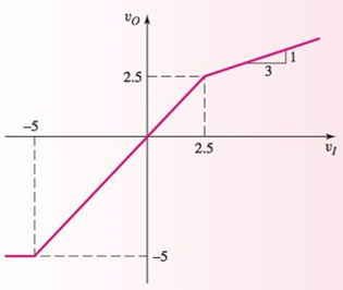
Figure 2.24 Figure for Exercise Ex 2.7
Expert Solution & Answer
Want to see the full answer?
Check out a sample textbook solution
Students have asked these similar questions
.I need the correct answer, and if it's wrong, please fix it
7. The midrange voltage gain of an amplifier is 100. The input RC circuit has a lower critical
frequency of 1 kHz. The actual voltage gain at f-100 Hz is 100.
10. In a high-pass filter, the roll-off region occurs above the critical frequency.
Solve this problem and show all of the work
Don't use ai to answer I will report you answer
Chapter 2 Solutions
MICROELECT. CIRCUIT ANALYSIS&DESIGN (LL)
Ch. 2 - Repeat Example 2.1 if the input voltage is...Ch. 2 - Consider the bridge circuit shown in Figure 2.6(a)...Ch. 2 - Assume the input signal to a rectifier circuit has...Ch. 2 - The input voltage to the halfwave rectifier in...Ch. 2 - Consider the circuit in Figure 2.4. The input...Ch. 2 - The circuit in Figure 2.5(a) is used to rectify a...Ch. 2 - The secondary transformer voltage of the rectifier...Ch. 2 - Determine the fraction (percent) of the cycle that...Ch. 2 - The Zener diode regulator circuit shown in Figure...Ch. 2 - Repeat Example 2.6 for rz=4 . Assume all other...
Ch. 2 - Consider the circuit shown in Figure 2.19. Let...Ch. 2 - Suppose the currentlimiting resistor in Example...Ch. 2 - Suppose the power supply voltage in the circuit...Ch. 2 - Design a parallelbased clipper that will yield the...Ch. 2 - Sketch the steadystate output voltage for the...Ch. 2 - Consider the circuit in Figure 2.23(a). Let R1=5k...Ch. 2 - Determine the steadystate output voltage O for the...Ch. 2 - Design a parallelbased clipper circuit that will...Ch. 2 - Consider the circuit shown in Figure 2.38, in...Ch. 2 - Consider the circuit shown in Figure 2.39. The...Ch. 2 - Repeat Example 2.11 for the case when R1=8k ,...Ch. 2 - The cutin voltage of each diode in the circuit...Ch. 2 - Prob. 2.12TYUCh. 2 - Consider the OR logic circuit shown in Figure...Ch. 2 - Consider the AND logic circuit shown in Figure...Ch. 2 - (a) Photons with an energy of hv=2eV are incident...Ch. 2 - Determine the value of resistance R required to...Ch. 2 - What characteristic of a diode is used in the...Ch. 2 - Prob. 2RQCh. 2 - Describe a simple fullwave diode rectifier circuit...Ch. 2 - Prob. 4RQCh. 2 - Prob. 5RQCh. 2 - Describe a simple Zener diode voltage reference...Ch. 2 - What effect does the Zener diode resistance have...Ch. 2 - What are the general characteristics of diode...Ch. 2 - Describe a simple diode clipper circuit that...Ch. 2 - Prob. 10RQCh. 2 - What one circuit element, besides a diode, is...Ch. 2 - Prob. 12RQCh. 2 - Describe a diode OR logic circuit. Compare a logic...Ch. 2 - Describe a diode AND logic circuit. Compare a...Ch. 2 - Describe a simple circuit that can be used to turn...Ch. 2 - Consider the circuit shown in Figure P2.1. Let...Ch. 2 - For the circuit shown in Figure P2.1, show that...Ch. 2 - A halfwave rectifier such as shown in Figure...Ch. 2 - Consider the battery charging circuit shown in...Ch. 2 - Figure P2.5 shows a simple fullwave battery...Ch. 2 - The fullwave rectifier circuit shown in Figure...Ch. 2 - The input signal voltage to the fullwave rectifier...Ch. 2 - The output resistance of the fullwave rectifier in...Ch. 2 - Repeat Problem 2.8 for the halfwave rectifier in...Ch. 2 - Consider the halfwave rectifier circuit shown in...Ch. 2 - The parameters of the halfwave rectifier circuit...Ch. 2 - The fullwave rectifier circuit shown in Figure...Ch. 2 - Consider the fullwave rectifier circuit in Figure...Ch. 2 - The circuit in Figure P2.14 is a complementary...Ch. 2 - Prob. 2.15PCh. 2 - A fullwave rectifier is to be designed using the...Ch. 2 - Prob. 2.17PCh. 2 - (a) Sketch o versus time for the circuit in Figure...Ch. 2 - Consider the circuit shown in Figure P2.19. The...Ch. 2 - Consider the Zener diode circuit shown in Figure...Ch. 2 - Consider the Zener diode circuit shown in Figure...Ch. 2 - In the voltage regulator circuit in Figure P2.21,...Ch. 2 - A Zener diode is connected in a voltage regulator...Ch. 2 - Consider the Zener diode circuit in Figure 2.19 in...Ch. 2 - Design a voltage regulator circuit such as shown...Ch. 2 - The percent regulation of the Zener diode...Ch. 2 - A voltage regulator is to have a nominal output...Ch. 2 - Consider the circuit in Figure P2.28. Let V=0 ....Ch. 2 - The secondary voltage in the circuit in Figure...Ch. 2 - The parameters in the circuit shown in Figure...Ch. 2 - Consider the circuit in Figure P2.31. Let V=0 (a)...Ch. 2 - Prob. 2.32PCh. 2 - Each diode cutin voltage is 0.7 V for the circuits...Ch. 2 - The diode in the circuit of Figure P2.34(a) has...Ch. 2 - Consider the circuits shown in Figure P2.35. Each...Ch. 2 - Plot O for each circuit in Figure P2.36 for the...Ch. 2 - Consider the parallel clipper circuit in Figure...Ch. 2 - A car’s radio may be subjected to voltage spikes...Ch. 2 - Sketch the steadystate output voltage O versus...Ch. 2 - Prob. D2.40PCh. 2 - Design a diode clamper to generate a steadystate...Ch. 2 - For the circuit in Figure P2.39(b), let V=0 and...Ch. 2 - Repeat Problem 2.42 for the circuit in Figure...Ch. 2 - The diodes in the circuit in Figure P2.44 have...Ch. 2 - In the circuit in Figure P2.45 the diodes have the...Ch. 2 - The diodes in the circuit in Figure P2.46 have the...Ch. 2 - Consider the circuit shown in Figure P2.47. Assume...Ch. 2 - The diode cutin voltage for each diode in the...Ch. 2 - Consider the circuit in Figure P2.49. Each diode...Ch. 2 - Assume V=0.7V for each diode in the circuit in...Ch. 2 - The cutin voltage of each diode in the circuit...Ch. 2 - Let V=0.7V for each diode in the circuit in Figure...Ch. 2 - For the circuit shown in Figure P2.54, let V=0.7V...Ch. 2 - Assume each diode cutin voltage is V=0.7V for the...Ch. 2 - If V=0.7V for the diode in the circuit in Figure...Ch. 2 - Let V=0.7V for the diode in the circuit in Figure...Ch. 2 - Each diode cutin voltage in the circuit in Figure...Ch. 2 - Let V=0.7V for each diode in the circuit shown in...Ch. 2 - Consider the circuit in Figure P2.61. The output...Ch. 2 - Consider the circuit in Figure P2.62. The output...Ch. 2 - Prob. 2.63PCh. 2 - Consider the circuit shown in Figure P2.64. The...Ch. 2 - The lightemitting diode in the circuit shown in...Ch. 2 - The parameters of D1 and D2 in the circuit shown...Ch. 2 - If the resistor in Example 2.12 is R=2 and the...Ch. 2 - Consider the photodiode circuit shown in Figure...Ch. 2 - Consider the fullwave bridge rectifier circuit....Ch. 2 - Design a simple dc voltage source using a...Ch. 2 - A clipper is to be designed such that O=2.5V for...Ch. 2 - Design a circuit to provide the voltage transfer...
Knowledge Booster


Learn more about
Need a deep-dive on the concept behind this application? Look no further. Learn more about this topic, electrical-engineering and related others by exploring similar questions and additional content below.Similar questions
- Don't use ai to answer I will report you answerarrow_forwardQ3/A unity-feedback system with the forward transfer function G(S)= K S(S+7) is operating with a closed-loop step response that has 15% overshoot. Do the following: a. Evaluate the steady-state error for a unit ramp input. b. Design a lag compensator to improve the steady-state error by a factor of 20 to get a new dominant closed-loop poles S-3.4+ j5.63. place the pole of the lag compensator at s=-0.01 c. Design a lag compensator using OP amp if R1= 100KS2 R2=10 KS2 and R3= 10Karrow_forwardQ2: (33 Marks) Design FBD for manufacturing system where a conveyor belt is used to move a cart through a tunnel for processing. The process begins when a worker presses a start push button located at the start of the conveyor. Once the start push button is pressed, the cart moves forward along the conveyor belt and enters the tunnel. When the cart reaches the end of the tunnel, it stops automatically and remains in place for 10-minutes to complete a required operation, such as cooling or drying. After the 10-minute delay, the cart automatically returns to the starting point where the worker is stationed. The system then waits for the worker to press the start push button again, at which point the process is repeated. Start PBO Stop PBO LSI 0 LS 2 Motorarrow_forward
- 1. Find the resolution, current and output voltage for a binary weighted resistor DAC of (applied binary word is (locoj), the resistor values R = 12 kQ, Rf = 6 k2 and VR = 12 V. 2. Convert the following 5-bit digital values (ble 10) to analog, using the R-2R ladder. Assume that the Vs = 10 V, R = Rf = 7 ksarrow_forwardK Q4/ For the unity-feedback system where G(s) = do the following: a. Plot the Nyquist diagram. (S+2)(S+4)(S+6) b. Use your Nyquist diagram to find the range of gain, K, for stabilityarrow_forwardQ6/ Answer (two) of the following question A For the following G(s), find analytical expressions for the magnitude and phase response and make a plot of the logmagnitude and the phase, using log-frequency in rad/s as the ordinate. G(S)=- 1 (S+2)(S+4)arrow_forward
- Q5 Given the system of Figure below, with dominant poles -5.415 t/10.57. design a PID controller so that the system can operate with a peak time that is two-thirds that of the uncompensated system at 20% overshoot to get and with zero steady-state error for a step input and KV= 5.7163sec and final K=4.6. R(s) + E(s) K(s + 8) (s+3)(x+6)(s + 10) C(s)arrow_forward".I need the correct answers with explanations" Answer True or False, then correct errors or explain if any: 1. The term pole in filter terminology refers to the feedback circuit. 2, A voltage shunt feedback with Ai-10, A-20, p 0.45, then Aif will be 1. 3. The integrator Op-Amp circuit can be used to produce square waves. 4. The equivalent circuit of the crystal oscillator is series and parallel (R, C) components. 5. The transistor in a class A power amplifier conducts for the entire input cycle. 6. Bypass capacitors in an amplifier determine the low and high-frequency responses. 7. The midrange voltage gain of an amplifier is 100. The input RC circuit has a lower critical frequency of 1 kHz. The actual voltage gain at f-100 Hz is 100. 8. The Bessel filter types produce almost ripple frequency response. 9. RC phase shift oscillators are based on both positive and negative feedback circuits. 10. In a high-pass filter, the roll-off region occurs above the critical frequency.arrow_forward".I need the correct answers with explanations" Answer True or False and correct errors if found: Marks) 1. The LC oscillator circuits are used to operate in low and moderate frequencies. 2. The voltage series feedback can increase both input and output impedances. 3. A two-pole Sallen-Key high-pass filter contains one capacitor and two resistors. 4. The main feature of a crystal oscillator is the high frequency operation that operates with optoelectronic effect. 5. The max. efficiency of the class B power amplifier is 50%. 6. The Q-point must be centered on the load line for maximum class AB output signal swing. 7. The differentiator Op-Amp can convert the triangle waveform into sinewave. 8. Class AB power amplifier eliminates crossover distortion found in pure class A. 9. RC-phase shift oscillators are based on positive feedback circuits. 10. Bypass capacitors in an amplifier determine the low and high-frequency responses.arrow_forward
- K Q2/A For the system G(s)= H(s)=1 9 (s+5)(s+2 )(s+5) a. Draw the Bode log-magnitude and phase plots. b. Find the range of K for stability from your Bode plots. c. Evaluate gain margia, phase margin, zero dB frequency, and 180° frequency from your Bode plots for K = 10,000.arrow_forwardPlease solve this question step by step handwritten solution and do not use ai or chat gpt pleasearrow_forward".I need the correct answers with explanations" Q1: What is the orientation of voltage regulation value (positive or negative) of alternator loaded by capacitive load? Explain the effect of armature reaction on voltage regulation for this load? Draw the load characteristics of alternator for capacitive, inductive, and inductive loads? Q2: A 2000 kVA,2200 V, 60 Hz,Y-connected alternator has a resistance of 0.25 between each pair of terminal. A field current of 80 A produces a short circuit current equal to full load current in each line. The same field current produces an e.m.f of 800 V(L-L) on open circuit .Determine the full load voltage regulation of alternator at unity p.f?arrow_forward
arrow_back_ios
SEE MORE QUESTIONS
arrow_forward_ios
Recommended textbooks for you

Diodes Explained - The basics how diodes work working principle pn junction; Author: The Engineering Mindset;https://www.youtube.com/watch?v=Fwj_d3uO5g8;License: Standard Youtube License