
MICROELECT. CIRCUIT ANALYSIS&DESIGN (LL)
4th Edition
ISBN: 9781266368622
Author: NEAMEN
Publisher: MCG
expand_more
expand_more
format_list_bulleted
Videos
Textbook Question
Chapter 2, Problem 2.66P
The parameters of
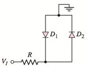
Figure P2.66
Expert Solution & Answer
Want to see the full answer?
Check out a sample textbook solution
Students have asked these similar questions
would anyone be able to tell me the amount of wire needed for this electrical plan in this house? and if possible would anyone be able to tell me the amount of any other materials needed (wire sizes, box sizes/styles)
Please show all steps
A plane wave propagating in the +z direction in medium 1 is normally incident to medium 2 located at
the z=0 plane as below. Both mediums are general, characterized by ( ε i, Mi, Ơi ).
tot
=
[ ει μη σ]
[ε, μη σε ]
Ex
Ex
tot
E₁₂ (z) = Ee
Ex
z=0
From conservation of energy: P₁AV'(z=0) + Piav'(z=0) = P2av²(z=0).
Using the above show for lossless media that: ( 1 - ||²) = (1/M2 )|T|² .
Chapter 2 Solutions
MICROELECT. CIRCUIT ANALYSIS&DESIGN (LL)
Ch. 2 - Repeat Example 2.1 if the input voltage is...Ch. 2 - Consider the bridge circuit shown in Figure 2.6(a)...Ch. 2 - Assume the input signal to a rectifier circuit has...Ch. 2 - The input voltage to the halfwave rectifier in...Ch. 2 - Consider the circuit in Figure 2.4. The input...Ch. 2 - The circuit in Figure 2.5(a) is used to rectify a...Ch. 2 - The secondary transformer voltage of the rectifier...Ch. 2 - Determine the fraction (percent) of the cycle that...Ch. 2 - The Zener diode regulator circuit shown in Figure...Ch. 2 - Repeat Example 2.6 for rz=4 . Assume all other...
Ch. 2 - Consider the circuit shown in Figure 2.19. Let...Ch. 2 - Suppose the currentlimiting resistor in Example...Ch. 2 - Suppose the power supply voltage in the circuit...Ch. 2 - Design a parallelbased clipper that will yield the...Ch. 2 - Sketch the steadystate output voltage for the...Ch. 2 - Consider the circuit in Figure 2.23(a). Let R1=5k...Ch. 2 - Determine the steadystate output voltage O for the...Ch. 2 - Design a parallelbased clipper circuit that will...Ch. 2 - Consider the circuit shown in Figure 2.38, in...Ch. 2 - Consider the circuit shown in Figure 2.39. The...Ch. 2 - Repeat Example 2.11 for the case when R1=8k ,...Ch. 2 - The cutin voltage of each diode in the circuit...Ch. 2 - Prob. 2.12TYUCh. 2 - Consider the OR logic circuit shown in Figure...Ch. 2 - Consider the AND logic circuit shown in Figure...Ch. 2 - (a) Photons with an energy of hv=2eV are incident...Ch. 2 - Determine the value of resistance R required to...Ch. 2 - What characteristic of a diode is used in the...Ch. 2 - Prob. 2RQCh. 2 - Describe a simple fullwave diode rectifier circuit...Ch. 2 - Prob. 4RQCh. 2 - Prob. 5RQCh. 2 - Describe a simple Zener diode voltage reference...Ch. 2 - What effect does the Zener diode resistance have...Ch. 2 - What are the general characteristics of diode...Ch. 2 - Describe a simple diode clipper circuit that...Ch. 2 - Prob. 10RQCh. 2 - What one circuit element, besides a diode, is...Ch. 2 - Prob. 12RQCh. 2 - Describe a diode OR logic circuit. Compare a logic...Ch. 2 - Describe a diode AND logic circuit. Compare a...Ch. 2 - Describe a simple circuit that can be used to turn...Ch. 2 - Consider the circuit shown in Figure P2.1. Let...Ch. 2 - For the circuit shown in Figure P2.1, show that...Ch. 2 - A halfwave rectifier such as shown in Figure...Ch. 2 - Consider the battery charging circuit shown in...Ch. 2 - Figure P2.5 shows a simple fullwave battery...Ch. 2 - The fullwave rectifier circuit shown in Figure...Ch. 2 - The input signal voltage to the fullwave rectifier...Ch. 2 - The output resistance of the fullwave rectifier in...Ch. 2 - Repeat Problem 2.8 for the halfwave rectifier in...Ch. 2 - Consider the halfwave rectifier circuit shown in...Ch. 2 - The parameters of the halfwave rectifier circuit...Ch. 2 - The fullwave rectifier circuit shown in Figure...Ch. 2 - Consider the fullwave rectifier circuit in Figure...Ch. 2 - The circuit in Figure P2.14 is a complementary...Ch. 2 - Prob. 2.15PCh. 2 - A fullwave rectifier is to be designed using the...Ch. 2 - Prob. 2.17PCh. 2 - (a) Sketch o versus time for the circuit in Figure...Ch. 2 - Consider the circuit shown in Figure P2.19. The...Ch. 2 - Consider the Zener diode circuit shown in Figure...Ch. 2 - Consider the Zener diode circuit shown in Figure...Ch. 2 - In the voltage regulator circuit in Figure P2.21,...Ch. 2 - A Zener diode is connected in a voltage regulator...Ch. 2 - Consider the Zener diode circuit in Figure 2.19 in...Ch. 2 - Design a voltage regulator circuit such as shown...Ch. 2 - The percent regulation of the Zener diode...Ch. 2 - A voltage regulator is to have a nominal output...Ch. 2 - Consider the circuit in Figure P2.28. Let V=0 ....Ch. 2 - The secondary voltage in the circuit in Figure...Ch. 2 - The parameters in the circuit shown in Figure...Ch. 2 - Consider the circuit in Figure P2.31. Let V=0 (a)...Ch. 2 - Prob. 2.32PCh. 2 - Each diode cutin voltage is 0.7 V for the circuits...Ch. 2 - The diode in the circuit of Figure P2.34(a) has...Ch. 2 - Consider the circuits shown in Figure P2.35. Each...Ch. 2 - Plot O for each circuit in Figure P2.36 for the...Ch. 2 - Consider the parallel clipper circuit in Figure...Ch. 2 - A car’s radio may be subjected to voltage spikes...Ch. 2 - Sketch the steadystate output voltage O versus...Ch. 2 - Prob. D2.40PCh. 2 - Design a diode clamper to generate a steadystate...Ch. 2 - For the circuit in Figure P2.39(b), let V=0 and...Ch. 2 - Repeat Problem 2.42 for the circuit in Figure...Ch. 2 - The diodes in the circuit in Figure P2.44 have...Ch. 2 - In the circuit in Figure P2.45 the diodes have the...Ch. 2 - The diodes in the circuit in Figure P2.46 have the...Ch. 2 - Consider the circuit shown in Figure P2.47. Assume...Ch. 2 - The diode cutin voltage for each diode in the...Ch. 2 - Consider the circuit in Figure P2.49. Each diode...Ch. 2 - Assume V=0.7V for each diode in the circuit in...Ch. 2 - The cutin voltage of each diode in the circuit...Ch. 2 - Let V=0.7V for each diode in the circuit in Figure...Ch. 2 - For the circuit shown in Figure P2.54, let V=0.7V...Ch. 2 - Assume each diode cutin voltage is V=0.7V for the...Ch. 2 - If V=0.7V for the diode in the circuit in Figure...Ch. 2 - Let V=0.7V for the diode in the circuit in Figure...Ch. 2 - Each diode cutin voltage in the circuit in Figure...Ch. 2 - Let V=0.7V for each diode in the circuit shown in...Ch. 2 - Consider the circuit in Figure P2.61. The output...Ch. 2 - Consider the circuit in Figure P2.62. The output...Ch. 2 - Prob. 2.63PCh. 2 - Consider the circuit shown in Figure P2.64. The...Ch. 2 - The lightemitting diode in the circuit shown in...Ch. 2 - The parameters of D1 and D2 in the circuit shown...Ch. 2 - If the resistor in Example 2.12 is R=2 and the...Ch. 2 - Consider the photodiode circuit shown in Figure...Ch. 2 - Consider the fullwave bridge rectifier circuit....Ch. 2 - Design a simple dc voltage source using a...Ch. 2 - A clipper is to be designed such that O=2.5V for...Ch. 2 - Design a circuit to provide the voltage transfer...
Knowledge Booster


Learn more about
Need a deep-dive on the concept behind this application? Look no further. Learn more about this topic, electrical-engineering and related others by exploring similar questions and additional content below.Similar questions
- A plane wave propagating in the +z direction in medium 1 is normally incident to medium 2 located at the z=0 plane as below. Both mediums are general, characterized by ( ε i, Hi, σ¡ ). [ ει μη σ] Ex [ ει μη ση ] Ex tot E₁₂ (z) = E'₁e¹² -122 E(z) = Ee+ E₁₁₁² E₁x z=0 1. Specify the electric field reflection coefficient г and transmission coefficient T: E ΓΔ E E TA EL 2. Show that T=1+г. Can the transmitted electric field amplitude in region 2 be LARGER than the incident electric field amplitude? 3. Determine expressions for P₁AV'(z), PIAV'(z) and P2AV'(z) (note the sign for the reflected power direction should be (-z).arrow_forward2) In the ideal transformer circuit shown below find Vo and the complex power supplied by the source. 292 www b 1:4 16 Ω ww + + 240/0° V rms -12492arrow_forward3) In the ideal autotransformer circuit shown below find 11, 12 and lo. Find the average power delivered to the load. (hint: write KVL for both sides) 20/30° V(+ 2-1602 200 turns V₂ 10 + j40 Ω 80 turns V₁arrow_forward
- 1) Find Vo in the following circuit. Assume the mesh currents are clockwise. ΠΩ Ω ΖΩ ww 1Ω ww 24/0° (± 6 Ω j4 Ω 1Ω +arrow_forwardPlease show all stepsarrow_forward11-3) similar to Lathi & Ding, Prob. P.6.8-1 Consider the carrier modulator shown in the figure below, which transmits a binary carrier signal. The baseband generator uses polar NRZ signaling with rectangular pulses. The data rate is 8 Mbit/s. (a) If the modulator generates a binary PSK signal, what is the bandwidth of the modulated output? (b) If the modulator generates FSK with the difference fel - fco = 6 MHz (cf. Fig 6.32c), determine the modulated signal bandwidth. Binary data source Baseband signal generator Modulated output Modulator N-E---arrow_forward
- Choose the best answer for each: 1. What does SRAM use to store data? 。 a) Capacitors ob) Latches 。 c) Flip-flops od) Transistors 2. Which RAM type requires refreshing? o a) SRAM ob) DRAM 。 c) ROM od) Flash 3. What type of memory retains data only while power is on? a) ROM 。 b) EEPROM o c) DRAM od) Flash 4. How many addresses can a 15-bit address bus handle? o a) 32k • b) 64k o c) 16k od) lk 5. What operation occurs when data is copied out of memory without erasing? oa) Write ob) Read o c) Refresh o d) Load 6. DRAM cells store bits using: a) Flip-flops 。 b) Capacitors c) Diodes od) Resistors 7. The cache located inside the CPU is: 。 a) L2 cache o b) LI cache °c) ROM od) HDD 8. SDRAM is synchronized with: o a) Cache ob) Data Bus c) System Clock od) Hard Disk 9. The bus that carries commands is called: o a) Data Bus b) Control Bus o c) Address Bus o d) Logic Bus 10. What is the main use of SRAM? o Disk storage o Cache o Main memory o Registers 11. The smallest addressable unit in…arrow_forwardQ4: A cache memory is 128k × 16. How many bytes can it store?arrow_forwardSketch the output of the analogue computer shown below and find its closest describing function [suppose any variable to find the DF] +1 ew2 HI e2 1.0 +21 LO SJ eo SJ ew LO 1.0 +|e1| HI -1 ew1 ek(1 + e。) |e1| k = 1+|e1| Figure V-5 Feedback Limiter Behavior ROUNDED, DUE TO DIODE NONLINEARITY LIMIT VOLTAGE 409 DIODE CONDUCTS First, write the output transaction, then draw the output wave, and then find the Describing function. I need to solve the question step by step, with an explanation of each step.arrow_forward
arrow_back_ios
SEE MORE QUESTIONS
arrow_forward_ios
Recommended textbooks for you

 Electricity for Refrigeration, Heating, and Air C...Mechanical EngineeringISBN:9781337399128Author:Russell E. SmithPublisher:Cengage Learning
Electricity for Refrigeration, Heating, and Air C...
Mechanical Engineering
ISBN:9781337399128
Author:Russell E. Smith
Publisher:Cengage Learning
Three-Phase Half-Wave Rectifier Operation; Author: katkimshow;https://www.youtube.com/watch?v=Uhbr6tbMB9A;License: Standard Youtube License