MICROELECT. CIRCUIT ANALYSIS&DESIGN (LL)
4th Edition
ISBN: 9781266368622
Author: NEAMEN
Publisher: MCG
bartleby

Videos

Textbook Question
Book Icon
Chapter 2, Problem 2.52P

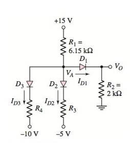
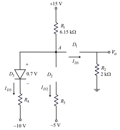
The cut−in voltage of each diode in the circuit shown in Figure P2.52 is V γ = 0.7 V . Determine I D 1 , I D 2 , I D 3 , and V A for (a) R 3 = 14 k Ω , R 4 = 24 k Ω ; (b) R 3 = 3.3 k Ω , R 4 = 5.2 k Ω ; and (c) R 3 = 3.3 k Ω , R 4 = 1.32 k Ω .
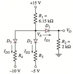
Chapter 2, Problem 2.52P, The cutin voltage of each diode in the circuit shown in Figure P2.52 is V=0.7V . Determine
Figure P2.52

(a)

Expert Solution
Check Mark
To determine

The values of ID1,ID2,ID3, and VA 

Answer to Problem 2.52P

The current flowing through diodes is

  ID3=0.5 mA

  ID2=0.5 mA , ID1=1 mA and VA=2.7 V

Explanation of Solution

Given:

  MICROELECT. CIRCUIT ANALYSIS&DESIGN (LL), Chapter 2, Problem 2.52P , additional homework tip  1

  R3=14kΩ R4=24kΩ 

Calculation:

The cut-in voltage for each diode is, Vγ=0.7V

Assume all diodes are ON.

Draw the circuit diagram with node voltages and cut-in voltages.
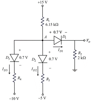
  MICROELECT. CIRCUIT ANALYSIS&DESIGN (LL), Chapter 2, Problem 2.52P , additional homework tip  2

Apply Kirchhoff’s current law node A.

  VA156.15k+VA0.72k+VA0.7(5)R3+VA0.7(10)R4=0VA156.15k+VA0.72k+VA+4.3R3+VA+9.3R4=0

Substitute 14kΩ for R3 and 24kΩ for R4 .

  VA156.15k+VA0.72k+VA+4.314k+VA+9.324k=0VA156.15+VA0.72+VA+4.314+VA+9.324=0(16.15+12+114+124)VA156.150.72+4.314+9.324=00.7756VA2.094=0VA=2.7 V

Therefore, the voltage at node A, VA is 2.7 V

Calculate the current flowing through diode, D1 .

  ID1=VA0.72k

Substitute 2.7V for VA .

  ID1=2.70.72k=22k=1 mA

Therefore, the current flowing through diode D1, is ID1=1 mA .

Calculate the current flowing through diode, D2 .

  ID2=VA0.7(5)R3

Substitute 2.7V for VA and 14 kΩ for R3 .

  ID2=2.70.7+514k=714k=0.5 mA

Therefore, the current flowing through diode D2, is ID2=0.5 mA .

Calculate the current flowing through diode, D3 .

  ID3=VA0.7(10)R4

Substitute 2.7V for VA and 24 kΩ for R4 .

  ID3=2.70.7+1024k=1224k=0.5 mA

Therefore, the current flowing through diodes is ID3=0.5 mA

Conclusion:

Therefore, the current flowing through diodes is

  ID3=0.5 mA

  ID2=0.5 mA , ID1=1 mA and VA=2.7 V

(b)

Expert Solution
Check Mark
To determine

The values of ID1,ID2,ID3, and VA 

Answer to Problem 2.52P

The current flowing through diodes is VA=0.991V , ID10 A , ID2=1.003 mA and ID3=1.6 mA

Explanation of Solution

Given:

  R3=3.3kΩ R4=5.2kΩ 

Calculation:

Assume diode D1 is OFF and remaining diodes are ON.

Draw the circuit diagram with node voltages and cut-in voltages.
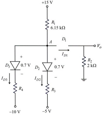
  MICROELECT. CIRCUIT ANALYSIS&DESIGN (LL), Chapter 2, Problem 2.52P , additional homework tip  3

Apply Kirchhoff’s current law node A.

  VA156.15k+VA0.7(5)R3+VA0.7(10)R4=0VA156.15k+VA+4.3R3+VA+9.3R4=0

Substitute 3.3kΩ for R3 and 5.2kΩ for R4 .

  VA156.15k+VA+4.33.3k+VA+9.35.2k=0VA156.15+VA+4.33.3+VA+9.35.2=0(16.15+13.3+15.2)VA156.15+4.33.3+9.35.2=00.6579VA+0.6525=0VA=0.65250.6579=0.991V

Therefore, the voltage at node A, VA is 0.991V

The diode D1 is reverse biased. Therefore, the current flowing through diode D1 is zero.

That is, ID1=0 A .

Therefore, the current flowing through diode D1,

  ID10 A

Calculate the current flowing through diode, D2 .

  ID2=VA0.7(5)R3

Substitute 0.991V for VA and 3.3 kΩ for R3 .

  ID2=0.9910.7+53.3k=3.3093.3k=1.003 mA

Therefore, the current flowing through diode D2, is ID2=1.003 mA .

Calculate the current flowing through diode, D3 .

  ID3=VA0.7(10)R4

Substitute 0.991V for VA and 5.2 kΩ for R4 .

  ID3=0.9910.7+105.2k=8.3095.2k=1.6 mA

Therefore, the current flowing through diode D3, is ID3=1.6 mA .

Conclusion:

Therefore, the current flowing through diodes is VA=0.991V , ID10 A , ID2=1.003 mA and ID3=1.6 mA

(c)

Expert Solution
Check Mark
To determine

The values of ID1,ID2,ID3, and VA 

Answer to Problem 2.52P

The current flowing through diodes is VA=5V , ID1=0 A , ID2=0 A

  ID3=3.25 mA

Explanation of Solution

Given:

  R3=3.3kΩR4=1.32kΩ

Calculation:

Assume diode D1 and D2 are OFF and diode D3 is ON.

Draw the circuit diagram with node voltages and cut-in voltages.
  MICROELECT. CIRCUIT ANALYSIS&DESIGN (LL), Chapter 2, Problem 2.52P , additional homework tip  4

Apply Kirchhoff’s current law node A.

  VA156.15k+VA0.7(10)R4=0VA156.15k+VA+9.3R4=0

Substitute 1.32kΩ for R4 .

  VA156.15k+VA+9.31.32k=0VA156.15+VA+9.31.32=0(16.15+11.32)VA156.15+9.31.32=00.92VA+4.606=0VA=5V

Therefore, the voltage at node A, VA is 5V .

The Diode D1 and D2 are reverse biased. Therefore, the current flowing through diode D1 is zero.

That is, ID1=0 A .

Therefore, the current flowing through diode D1,ID1 is 0 A.

The current flowing through the diode, D2 is zero.

That is,

  ID2=0 A.

Therefore, the current flowing through diode D2,ID2 is 0 A.

Calculate the current flowing through diode, D3 .

  ID3=VA0.7(10)R4

Substitute 5V for VA and 1.32 kΩ for R4 .

  ID3=50.7+101.32k=4.31.32k=3.25 mA

Therefore, the current flowing through diode D3, is ID3=3.25 mA .

Conclusion:

Therefore, the current flowing through diodes is VA=5V , ID1=0 A , ID2=0 A

  ID3=3.25 mA

Want to see more full solutions like this?

Subscribe now to access step-by-step solutions to millions of textbook problems written by subject matter experts!
Students have asked these similar questions
Answer the following questions: 1- Write radiation resistance (R.) equation for infinitesimal dipole antenna. 2- Write the angle expression form of first null beam width (FNBW) for 2/2 dipole. 3- Define the Directivity of antenna. 4- Write radar cross section equation. 5- Write the input impedance (Z) expression of lossless transmission line.
The input reactance of an infinitesimal linear dipole of length 1/60 and radius a = x/200 is given by [In(/2a) - 11 X-120- tan(kl/2) Assuming the wire of the dipole is copper with a conductivity of 5.7 × 10'S/m. determine at f = 1 GHz the (a) loss resistance (b) radiation resistance (c) radiation efficiency input impedance
Q4- a) For the block diagram of control system shown below with its unit step response. Determine (K, a,damping ration, Maximum overshoot, Wn, Wd,ẞ, ts, tp, td, tr, and overall transfer function? C(1) ↑ 1.4 1.2 1 0.8 0.6 0.4 0.2 R(s) E(s) K C(s) $(s + α) 0.05 0.1 0.15 0.2 +2% -2%

Chapter 2 Solutions

MICROELECT. CIRCUIT ANALYSIS&DESIGN (LL)

Ch. 2 - Consider the circuit shown in Figure 2.19. Let...Ch. 2 - Suppose the currentlimiting resistor in Example...Ch. 2 - Suppose the power supply voltage in the circuit...Ch. 2 - Design a parallelbased clipper that will yield the...Ch. 2 - Sketch the steadystate output voltage for the...Ch. 2 - Consider the circuit in Figure 2.23(a). Let R1=5k...Ch. 2 - Determine the steadystate output voltage O for the...Ch. 2 - Design a parallelbased clipper circuit that will...Ch. 2 - Consider the circuit shown in Figure 2.38, in...Ch. 2 - Consider the circuit shown in Figure 2.39. The...Ch. 2 - Repeat Example 2.11 for the case when R1=8k ,...Ch. 2 - The cutin voltage of each diode in the circuit...Ch. 2 - Prob. 2.12TYUCh. 2 - Consider the OR logic circuit shown in Figure...Ch. 2 - Consider the AND logic circuit shown in Figure...Ch. 2 - (a) Photons with an energy of hv=2eV are incident...Ch. 2 - Determine the value of resistance R required to...Ch. 2 - What characteristic of a diode is used in the...Ch. 2 - Prob. 2RQCh. 2 - Describe a simple fullwave diode rectifier circuit...Ch. 2 - Prob. 4RQCh. 2 - Prob. 5RQCh. 2 - Describe a simple Zener diode voltage reference...Ch. 2 - What effect does the Zener diode resistance have...Ch. 2 - What are the general characteristics of diode...Ch. 2 - Describe a simple diode clipper circuit that...Ch. 2 - Prob. 10RQCh. 2 - What one circuit element, besides a diode, is...Ch. 2 - Prob. 12RQCh. 2 - Describe a diode OR logic circuit. Compare a logic...Ch. 2 - Describe a diode AND logic circuit. Compare a...Ch. 2 - Describe a simple circuit that can be used to turn...Ch. 2 - Consider the circuit shown in Figure P2.1. Let...Ch. 2 - For the circuit shown in Figure P2.1, show that...Ch. 2 - A halfwave rectifier such as shown in Figure...Ch. 2 - Consider the battery charging circuit shown in...Ch. 2 - Figure P2.5 shows a simple fullwave battery...Ch. 2 - The fullwave rectifier circuit shown in Figure...Ch. 2 - The input signal voltage to the fullwave rectifier...Ch. 2 - The output resistance of the fullwave rectifier in...Ch. 2 - Repeat Problem 2.8 for the halfwave rectifier in...Ch. 2 - Consider the halfwave rectifier circuit shown in...Ch. 2 - The parameters of the halfwave rectifier circuit...Ch. 2 - The fullwave rectifier circuit shown in Figure...Ch. 2 - Consider the fullwave rectifier circuit in Figure...Ch. 2 - The circuit in Figure P2.14 is a complementary...Ch. 2 - Prob. 2.15PCh. 2 - A fullwave rectifier is to be designed using the...Ch. 2 - Prob. 2.17PCh. 2 - (a) Sketch o versus time for the circuit in Figure...Ch. 2 - Consider the circuit shown in Figure P2.19. The...Ch. 2 - Consider the Zener diode circuit shown in Figure...Ch. 2 - Consider the Zener diode circuit shown in Figure...Ch. 2 - In the voltage regulator circuit in Figure P2.21,...Ch. 2 - A Zener diode is connected in a voltage regulator...Ch. 2 - Consider the Zener diode circuit in Figure 2.19 in...Ch. 2 - Design a voltage regulator circuit such as shown...Ch. 2 - The percent regulation of the Zener diode...Ch. 2 - A voltage regulator is to have a nominal output...Ch. 2 - Consider the circuit in Figure P2.28. Let V=0 ....Ch. 2 - The secondary voltage in the circuit in Figure...Ch. 2 - The parameters in the circuit shown in Figure...Ch. 2 - Consider the circuit in Figure P2.31. Let V=0 (a)...Ch. 2 - Prob. 2.32PCh. 2 - Each diode cutin voltage is 0.7 V for the circuits...Ch. 2 - The diode in the circuit of Figure P2.34(a) has...Ch. 2 - Consider the circuits shown in Figure P2.35. Each...Ch. 2 - Plot O for each circuit in Figure P2.36 for the...Ch. 2 - Consider the parallel clipper circuit in Figure...Ch. 2 - A car’s radio may be subjected to voltage spikes...Ch. 2 - Sketch the steadystate output voltage O versus...Ch. 2 - Prob. D2.40PCh. 2 - Design a diode clamper to generate a steadystate...Ch. 2 - For the circuit in Figure P2.39(b), let V=0 and...Ch. 2 - Repeat Problem 2.42 for the circuit in Figure...Ch. 2 - The diodes in the circuit in Figure P2.44 have...Ch. 2 - In the circuit in Figure P2.45 the diodes have the...Ch. 2 - The diodes in the circuit in Figure P2.46 have the...Ch. 2 - Consider the circuit shown in Figure P2.47. Assume...Ch. 2 - The diode cutin voltage for each diode in the...Ch. 2 - Consider the circuit in Figure P2.49. Each diode...Ch. 2 - Assume V=0.7V for each diode in the circuit in...Ch. 2 - The cutin voltage of each diode in the circuit...Ch. 2 - Let V=0.7V for each diode in the circuit in Figure...Ch. 2 - For the circuit shown in Figure P2.54, let V=0.7V...Ch. 2 - Assume each diode cutin voltage is V=0.7V for the...Ch. 2 - If V=0.7V for the diode in the circuit in Figure...Ch. 2 - Let V=0.7V for the diode in the circuit in Figure...Ch. 2 - Each diode cutin voltage in the circuit in Figure...Ch. 2 - Let V=0.7V for each diode in the circuit shown in...Ch. 2 - Consider the circuit in Figure P2.61. The output...Ch. 2 - Consider the circuit in Figure P2.62. The output...Ch. 2 - Prob. 2.63PCh. 2 - Consider the circuit shown in Figure P2.64. The...Ch. 2 - The lightemitting diode in the circuit shown in...Ch. 2 - The parameters of D1 and D2 in the circuit shown...Ch. 2 - If the resistor in Example 2.12 is R=2 and the...Ch. 2 - Consider the photodiode circuit shown in Figure...Ch. 2 - Consider the fullwave bridge rectifier circuit....Ch. 2 - Design a simple dc voltage source using a...Ch. 2 - A clipper is to be designed such that O=2.5V for...Ch. 2 - Design a circuit to provide the voltage transfer...
Knowledge Booster
Background pattern image
Electrical Engineering
Learn more about
Need a deep-dive on the concept behind this application? Look no further. Learn more about this topic, electrical-engineering and related others by exploring similar questions and additional content below.
Similar questions
SEE MORE QUESTIONS
Recommended textbooks for you
Text book image
Introductory Circuit Analysis (13th Edition)
Electrical Engineering
ISBN:9780133923605
Author:Robert L. Boylestad
Publisher:PEARSON
Text book image
Delmar's Standard Textbook Of Electricity
Electrical Engineering
ISBN:9781337900348
Author:Stephen L. Herman
Publisher:Cengage Learning
Text book image
Programmable Logic Controllers
Electrical Engineering
ISBN:9780073373843
Author:Frank D. Petruzella
Publisher:McGraw-Hill Education
Text book image
Fundamentals of Electric Circuits
Electrical Engineering
ISBN:9780078028229
Author:Charles K Alexander, Matthew Sadiku
Publisher:McGraw-Hill Education
Text book image
Electric Circuits. (11th Edition)
Electrical Engineering
ISBN:9780134746968
Author:James W. Nilsson, Susan Riedel
Publisher:PEARSON
Text book image
Engineering Electromagnetics
Electrical Engineering
ISBN:9780078028151
Author:Hayt, William H. (william Hart), Jr, BUCK, John A.
Publisher:Mcgraw-hill Education,
Three-Phase Half-Wave Rectifier Operation; Author: katkimshow;https://www.youtube.com/watch?v=Uhbr6tbMB9A;License: Standard Youtube License