MICROELECT. CIRCUIT ANALYSIS&DESIGN (LL)
4th Edition
ISBN: 9781266368622
Author: NEAMEN
Publisher: MCG
bartleby

Concept explainers

bartleby

Videos

Textbook Question
Book Icon
Chapter 2, Problem 2.51P

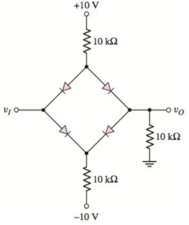
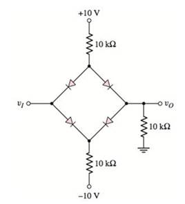
Assume V γ = 0.7 V for each diode in the circuit in Figure P251. Plot υ O versus υ I for 10 υ I + 10 V .

Chapter 2, Problem 2.51P, Assume V=0.7V for each diode in the circuit in Figure P251. Plot O versus I for 10I+10V . Figure
Figure P2.51

Expert Solution & Answer
Check Mark
To determine

To plot: The output voltage, v0 versus the input voltage, v1 .

Explanation of Solution

Given:

  Vγ=0.7V

  10Vv1+10V

  MICROELECT. CIRCUIT ANALYSIS&DESIGN (LL), Chapter 2, Problem 2.51P , additional homework tip  1

Calculation:

Case 1:

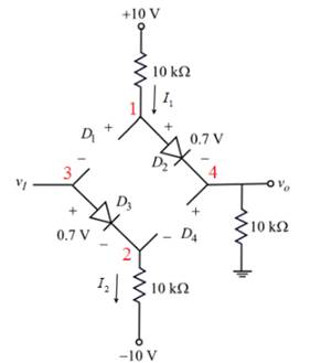
Assume that diodes D1 and D4 are reverse biased and diodes D2 and D3 are forward blased as shown in Figure 1.
  MICROELECT. CIRCUIT ANALYSIS&DESIGN (LL), Chapter 2, Problem 2.51P , additional homework tip  2

Figure 1

Apply the Kirchhoff’s voltage to the outer branch of the circuit shown in figure 1.

  10+(10K)I1+0.7+(10k)I1=0

Therefore,

  I1=100.710k+10k=9.320k=0.465mA

The voltage at node 4 of the circuit shown in figure 1 is,

  v0=I1(10k)=(0.465×10³)(10k)=4.65V

The voltage at node 1 of the circuit shown in figure 1 is,

  v1=0.7+I1(10k)=0.7+(0.465×10³)(10k)=5.35V

Apply the Kirchhoff’s voltage to the input branch of the circuit shown in figure 1 .

  v1+0.7+(10k)I210=0

Therefore,

  I2=100.7+v110k=9.3+v110k

The voltage at node 2 is,

  v2=I2(10k)10=(9.3+v110k)(10k)10=9.3+v110=v10.7

The diode D1 gets reverse biased if,

  v1v3<0.75.35v1<0.7v1>4.65V

The diode D4 gets reverse biased if,

  v0v2<0.74.65(v10.7)<0.74.65v1+0.7<0.7v1>4.65V

Therefore, diodes D1 and D4 gets reverse biased for v1>4.65V .

The output voltage is constant for v1>4.65V .

  v0=4.65V .

Case 2:

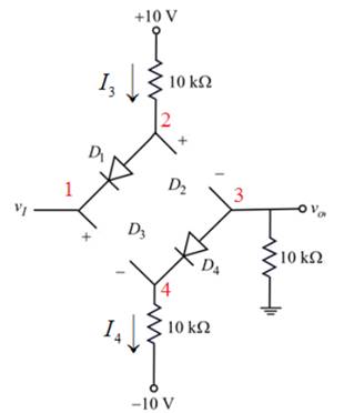
Assume that diodes D1 and D4 are forward biased and diodes D2 and D3 are reverse biased as shown in Figure 2.

  MICROELECT. CIRCUIT ANALYSIS&DESIGN (LL), Chapter 2, Problem 2.51P , additional homework tip  3

Figure 2

Apply the Kirchhoff’s voltage to the outer branch of the circuit shown in figure 2.

  (10k)I4+0.7+(10k)I410=0I4=100.710k+10k=9.320mA=0.465mA

The voltage at node 3 of the circuit shown in figure 2 is,

  v0=I4(10k)=(0.465×10³)(10k)=4.65V

The voltage at node 4 of the circuit shown in figure 2 is,

  v4=I4(10k)10=(0.465×10³)(10k)10=5.35V

Apply the Kirchhoff’s voltage to the input branch of the circuit shown in figure 2.

  10+(10k)I3+0.7+v1=0

Therefore,

  I3=100.7v110k=9.3v110k

The voltage at node 2 of the circuit shown in figure 2 is,

  v2=I3(10k)+10=(9.3v110k)(10k)+10=9.3+v1+10=v1+0.7

The diode D2 gets reverse biased if,

  v2v0<0.7(v1+0.7)(4.65)<0.7v1<4.65V

The diode D3 gets reverse biased if,

  v1v4<0.7v1(5.35)<0.7v1+5.35<0.7v1<4.65V

Therefore, diodes D2 and D3 gets reverse biased for v1<4.65V

Therefore, the output voltage is constant for v1<4.65V .

  v0=4.65V .

Case 3:

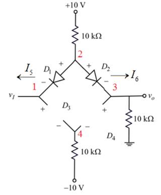
Assume that diodes D1 and D2 are forward biased and diodes D3 and D4 are reverse biased as shown in Figure 3.

  MICROELECT. CIRCUIT ANALYSIS&DESIGN (LL), Chapter 2, Problem 2.51P , additional homework tip  4

Figure 3

Apply the Kirchhoff’s current law at node 2 of the circuit shown in figure 3.

  I5+I6=10v210kI5+v20.710k=10v210kI5=10v2v2+0.710k=10.72v210k

The diode D1 gets forward biased if,

  I5010.72v110k0v15.35V

Apply the Kirchhoff’s voltage law to the input branch of the circuit shown in figure 3.

  v2+0.7+v1=0v2=0.7+v1 …….(1)

The voltage across diode D2 is,

  v2v0=2.7v0=v20.7

Consider equation(1).

Rewrite as,

  v0=(0.7+v1)0.7=v1

Therefore, the output voltage is,

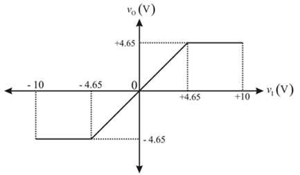
  v0={4.65V,v1<4.65Vv1,4.65Vv14.65V4.65V,v1>4.65V

Therefore, plot v0 versus v1 as shown in figure 4.

  MICROELECT. CIRCUIT ANALYSIS&DESIGN (LL), Chapter 2, Problem 2.51P , additional homework tip  5

Conclusion:

Therefore, plot of v0 versus v1 is drawn as shown in Figure 4.

Want to see more full solutions like this?

Subscribe now to access step-by-step solutions to millions of textbook problems written by subject matter experts!
Students have asked these similar questions
The input reactance of an infinitesimal linear dipole of length A/60 and radius a=A/200 is given by Xin = – 120 [In(€/a) — 1] tan(ke) Assuming the wire of the dipole is copper with a conductivity of 5.7 x 10' S/m, determine at f = 1 GHz the (a) loss resistance (b) radiation resistance (c) radiation efficiency (d) VSWR when the antenna is connected to a 50-ohm line
Example Solve the octic polynomial 2x⁸-9x⁷+20x⁶-33x⁵+46x⁴-66x³+80x²-72x+32=0 Solution Divide by x⁴ 2x⁴-9x³+20x²-33x+46-66/x + 80/x² - 72/x³ + 32/x⁴=0 Combine and bring terms 2(x⁴+16/x⁴) - 9(x³+8/x³) +20(x²+4/x²)-33(x+2/x) + 46= 0 Let use substitution Let x+2/x =u (x+2/x)²= u² x²+2x*2/x + 4/x² = u² x²+4/x²= u²-4 (x+2/x)³= x³+8/x³+3x*2/x(x+2/x) u³= x³+8/x²+6u x³+8/x³= u³-6u (x²+4/x²)²= x⁴+2x²*4/x² + 16/x⁴ (u²-4)²= x⁴+16/x⁴ + 8 x⁴+16/x⁴ = (u²-4)²-8 x⁴+16/x⁴ = u⁴-8u²+8 2(u⁴-8u²+8)-9(u³-6u)+20(u²-4)-33u+46=0 Expand and simplify 2u⁴-9u³+4u²+21u-18=0 After checking (u-1)(u-2) Are factors Then 2u²-3u-9=0 u=3, u=-3/2 Assignment question Solve the octic polynomial 2s⁸+s⁷+2s⁶-31s⁴-16s³-32s²-160=0 using the above example question, please explain in detail
b) Another waveform g(t) is defined by =0 t≥0, α>0 otherwise g(t)= At exp(-at) and is plotted in Figure 1 (for representative values of 4 = 1 and α = 1). g(t) 0.4T 0.3+ 0.2 0.1+ 2 0 2 Figure 1 8 c) Show that its amplitude spectrum is |G(@)| = - A (a²+0²)² Describe briefly, with the aid of labelled sketches, how changing a affects the waveform in both the time and frequency domains. d) Deduce the Fourier transform H(@) of h(t) = g(t)+g(t+b)+g(t-b) and calculate its DC amplitude H(0).

Chapter 2 Solutions

MICROELECT. CIRCUIT ANALYSIS&DESIGN (LL)

Ch. 2 - Consider the circuit shown in Figure 2.19. Let...Ch. 2 - Suppose the currentlimiting resistor in Example...Ch. 2 - Suppose the power supply voltage in the circuit...Ch. 2 - Design a parallelbased clipper that will yield the...Ch. 2 - Sketch the steadystate output voltage for the...Ch. 2 - Consider the circuit in Figure 2.23(a). Let R1=5k...Ch. 2 - Determine the steadystate output voltage O for the...Ch. 2 - Design a parallelbased clipper circuit that will...Ch. 2 - Consider the circuit shown in Figure 2.38, in...Ch. 2 - Consider the circuit shown in Figure 2.39. The...Ch. 2 - Repeat Example 2.11 for the case when R1=8k ,...Ch. 2 - The cutin voltage of each diode in the circuit...Ch. 2 - Prob. 2.12TYUCh. 2 - Consider the OR logic circuit shown in Figure...Ch. 2 - Consider the AND logic circuit shown in Figure...Ch. 2 - (a) Photons with an energy of hv=2eV are incident...Ch. 2 - Determine the value of resistance R required to...Ch. 2 - What characteristic of a diode is used in the...Ch. 2 - Prob. 2RQCh. 2 - Describe a simple fullwave diode rectifier circuit...Ch. 2 - Prob. 4RQCh. 2 - Prob. 5RQCh. 2 - Describe a simple Zener diode voltage reference...Ch. 2 - What effect does the Zener diode resistance have...Ch. 2 - What are the general characteristics of diode...Ch. 2 - Describe a simple diode clipper circuit that...Ch. 2 - Prob. 10RQCh. 2 - What one circuit element, besides a diode, is...Ch. 2 - Prob. 12RQCh. 2 - Describe a diode OR logic circuit. Compare a logic...Ch. 2 - Describe a diode AND logic circuit. Compare a...Ch. 2 - Describe a simple circuit that can be used to turn...Ch. 2 - Consider the circuit shown in Figure P2.1. Let...Ch. 2 - For the circuit shown in Figure P2.1, show that...Ch. 2 - A halfwave rectifier such as shown in Figure...Ch. 2 - Consider the battery charging circuit shown in...Ch. 2 - Figure P2.5 shows a simple fullwave battery...Ch. 2 - The fullwave rectifier circuit shown in Figure...Ch. 2 - The input signal voltage to the fullwave rectifier...Ch. 2 - The output resistance of the fullwave rectifier in...Ch. 2 - Repeat Problem 2.8 for the halfwave rectifier in...Ch. 2 - Consider the halfwave rectifier circuit shown in...Ch. 2 - The parameters of the halfwave rectifier circuit...Ch. 2 - The fullwave rectifier circuit shown in Figure...Ch. 2 - Consider the fullwave rectifier circuit in Figure...Ch. 2 - The circuit in Figure P2.14 is a complementary...Ch. 2 - Prob. 2.15PCh. 2 - A fullwave rectifier is to be designed using the...Ch. 2 - Prob. 2.17PCh. 2 - (a) Sketch o versus time for the circuit in Figure...Ch. 2 - Consider the circuit shown in Figure P2.19. The...Ch. 2 - Consider the Zener diode circuit shown in Figure...Ch. 2 - Consider the Zener diode circuit shown in Figure...Ch. 2 - In the voltage regulator circuit in Figure P2.21,...Ch. 2 - A Zener diode is connected in a voltage regulator...Ch. 2 - Consider the Zener diode circuit in Figure 2.19 in...Ch. 2 - Design a voltage regulator circuit such as shown...Ch. 2 - The percent regulation of the Zener diode...Ch. 2 - A voltage regulator is to have a nominal output...Ch. 2 - Consider the circuit in Figure P2.28. Let V=0 ....Ch. 2 - The secondary voltage in the circuit in Figure...Ch. 2 - The parameters in the circuit shown in Figure...Ch. 2 - Consider the circuit in Figure P2.31. Let V=0 (a)...Ch. 2 - Prob. 2.32PCh. 2 - Each diode cutin voltage is 0.7 V for the circuits...Ch. 2 - The diode in the circuit of Figure P2.34(a) has...Ch. 2 - Consider the circuits shown in Figure P2.35. Each...Ch. 2 - Plot O for each circuit in Figure P2.36 for the...Ch. 2 - Consider the parallel clipper circuit in Figure...Ch. 2 - A car’s radio may be subjected to voltage spikes...Ch. 2 - Sketch the steadystate output voltage O versus...Ch. 2 - Prob. D2.40PCh. 2 - Design a diode clamper to generate a steadystate...Ch. 2 - For the circuit in Figure P2.39(b), let V=0 and...Ch. 2 - Repeat Problem 2.42 for the circuit in Figure...Ch. 2 - The diodes in the circuit in Figure P2.44 have...Ch. 2 - In the circuit in Figure P2.45 the diodes have the...Ch. 2 - The diodes in the circuit in Figure P2.46 have the...Ch. 2 - Consider the circuit shown in Figure P2.47. Assume...Ch. 2 - The diode cutin voltage for each diode in the...Ch. 2 - Consider the circuit in Figure P2.49. Each diode...Ch. 2 - Assume V=0.7V for each diode in the circuit in...Ch. 2 - The cutin voltage of each diode in the circuit...Ch. 2 - Let V=0.7V for each diode in the circuit in Figure...Ch. 2 - For the circuit shown in Figure P2.54, let V=0.7V...Ch. 2 - Assume each diode cutin voltage is V=0.7V for the...Ch. 2 - If V=0.7V for the diode in the circuit in Figure...Ch. 2 - Let V=0.7V for the diode in the circuit in Figure...Ch. 2 - Each diode cutin voltage in the circuit in Figure...Ch. 2 - Let V=0.7V for each diode in the circuit shown in...Ch. 2 - Consider the circuit in Figure P2.61. The output...Ch. 2 - Consider the circuit in Figure P2.62. The output...Ch. 2 - Prob. 2.63PCh. 2 - Consider the circuit shown in Figure P2.64. The...Ch. 2 - The lightemitting diode in the circuit shown in...Ch. 2 - The parameters of D1 and D2 in the circuit shown...Ch. 2 - If the resistor in Example 2.12 is R=2 and the...Ch. 2 - Consider the photodiode circuit shown in Figure...Ch. 2 - Consider the fullwave bridge rectifier circuit....Ch. 2 - Design a simple dc voltage source using a...Ch. 2 - A clipper is to be designed such that O=2.5V for...Ch. 2 - Design a circuit to provide the voltage transfer...
Knowledge Booster
Background pattern image
Electrical Engineering
Learn more about
Need a deep-dive on the concept behind this application? Look no further. Learn more about this topic, electrical-engineering and related others by exploring similar questions and additional content below.
Similar questions
SEE MORE QUESTIONS
Recommended textbooks for you
Text book image
Electric Motor Control
Electrical Engineering
ISBN:9781133702818
Author:Herman
Publisher:CENGAGE L
Diodes Explained - The basics how diodes work working principle pn junction; Author: The Engineering Mindset;https://www.youtube.com/watch?v=Fwj_d3uO5g8;License: Standard Youtube License