MICROELECT. CIRCUIT ANALYSIS&DESIGN (LL)
4th Edition
ISBN: 9781266368622
Author: NEAMEN
Publisher: MCG
bartleby

Videos

Textbook Question
Book Icon
Chapter 2, Problem 2.47P

Consider the circuit shown in Figure P2.47. Assume each diode cut−in voltage is V γ = 0.6 V . (a) Determine R 1 , R 2 , and R 3 such that I D 1 = 0.2 mA , I D 2 = 0.3 mA , and I D 3 = 0.5 mA . (b) Find V 1 , V 2 , and each diode current for R 1 = 10 k Ω , R 2 = 4 k Ω , and R 3 = 2.2 k Ω . (c) Repeat part (b) for R 1 = 3 k Ω , R 2 = 6 k Ω , and R 3 = 2.5 k Ω . (d) Repeat part (b) for R 1 = 6 k Ω , R 2 = 3 k Ω , and R 3 = 6 k Ω .
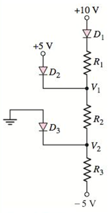
Chapter 2, Problem 2.47P, Consider the circuit shown in Figure P2.47. Assume each diode cutin voltage is V=0.6V . (a)
Figure P2.47

(a)

Expert Solution
Check Mark
To determine

The values of R1 , R2 , and R3

Answer to Problem 2.47P

The required values are,

  R1 is 25kΩ .

  R2 is 10kΩ .

  R3 is 4.4kΩ

Explanation of Solution

Given:

Diode’s cut-in voltage = Vγ=0.6V
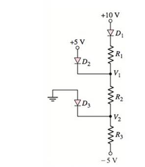
  ID1=0.2mA , ID2=0.3mA , and ID3=0.5mA

  MICROELECT. CIRCUIT ANALYSIS&DESIGN (LL), Chapter 2, Problem 2.47P , additional homework tip  1

Calculation:

Assume all diode are conducting.

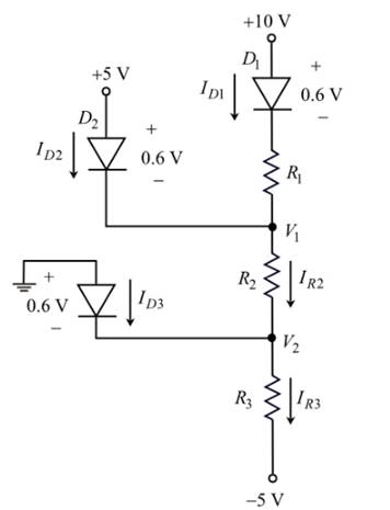
Draw the circuit diagram with node voltages and cut-in voltages.
  MICROELECT. CIRCUIT ANALYSIS&DESIGN (LL), Chapter 2, Problem 2.47P , additional homework tip  2

Figure 1

From Figure 1, the voltage at node V1 is,

  V1=50.6=4.4V

The voltage at node V2 is,

  V2=0.6V

Write the expression for current following through diode D1 .

  ID1=100V1R1

Substitute 0.2mA for ID1 and 4.4V for V1 .

  0.2×103=100.64.4R10.2×103=5R1R1=50.2×103=25kΩ

Therefore, the value of the resistor, R1 is 25kΩ .

Apply Kirchhoff’s current law at node V1 .

  IR2ID1ID2=0IR2=ID1+ID2

Substitute 0.2mA for ID1 and 0.3mA for ID2 .

  IR2=0.2mA+0.3mA=0.5mA

Calculate the value of resistor R2 using ohm’s law.

  IR2=V1V2R2

Substitute 0.5mA for IR2 , 4.4V For V1 and 0.6V for V2 .

  0.5×103=4.4(0.6)R2R2=50.5×10³R2=10kΩ

Therefore, the value of the resistor R2 is 10kΩ .

Apply Kirchhoff’s current law at node V2 .

  IR2ID3+IR3=0IR3=IR2+ID3

Substitute 0.5mA for IR2 and 0.5mA for ID3 .

  IR3=0.5mA+0.5mA=1mA

Calculate the value of resistor R3 using ohm’s law.

  R3=V2(5)IR3

Substitute 1mA for IR3 and 0.6V for V2 .

  R3=0.6(5)1×103=4.41×103=4.4kΩ

Therefore, the value of the resistor, R3 is 4.4kΩ

Conclusion:

Therefore, the required values are R1 is 25kΩ , R2 is 10kΩ and R3 is 4.4kΩ

(b)

Expert Solution
Check Mark
To determine

To find: The values of V1 , V2 and diode current for each.

Answer to Problem 2.47P

The required values are,

  V1 is 4.4V .

  V2 is 0.6V

  ID3 is 0.75mA

  ID2 is 0.75mA

  ID1 is 0.5mA

Explanation of Solution

Given:

Diode’s cut-in volt- age is Vγ=0.6V
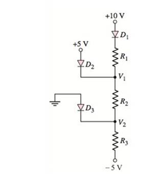
  R1=10kΩ , R2=4kΩ , and R3=2.2kΩ .

  MICROELECT. CIRCUIT ANALYSIS&DESIGN (LL), Chapter 2, Problem 2.47P , additional homework tip  3

Calculation:

Assume at diodes are conducting.

From Figure 1, the voltage at node V1 is,

  V1=50.6=4.4V

The voltage at node V2 is,

  V2=0.6V

Calculate the current, ID1 .

  ID1=100.6V1R1

Substitute 10kΩ for R1 and 4.4V for V1 .

  ID1=100.64.410×103=510×103=0.5mA

Therefore, the current following through diode D1 , ID1 is 0.5mA .

Calculate the current following through resistor R2 .

  IR2=V1V2R2

Substitute 4kΩ for R2 , 4.4V for V1 and 0.6V for V2 .

  IR2=4.4(0.6)4×103=54×103=1.25mA

Apply Kirchhoff’s current law at node V1 .

  IR2ID1ID2=0ID2=IR2ID1

Substitute 0.5mA for ID1 and 1.25mA for IR2 .

  ID2=1.25mA0.5mA=0.75mA

Therefore, the current following diode D2 , ID2 is 0.75mA .

Calculate the current following through resistor, R3 .

  IR3=V2(5)R3

Substitute 2.2kΩ for R3 and 0.6V for V2 .

  IR3=0.6+52.2×103=4.42.2×103=2mA

Apply Kirchhoff’s current law at node V2 .

  IR2ID3+IR3=0ID3=IR3IR2

Substitute 1.25mA for IR2 and 2mA for IR3 .

  ID3=2mA1.25mA=0.75mA

Therefore, the current following diode D3 , ID3 is 0.75mA .

Conclusion:

Therefore, the required values are V1 is 4.4V , V2 is 0.6V , ID3 is 0.75mA , ID2 is 0.75mA and ID1 is 0.5mA

(c)

Expert Solution
Check Mark
To determine

To find: The values of V1 , V2 and diode current for each.

Answer to Problem 2.47P

The require values are

  ID2 is 0A .

  V1 is 6.07V

  V2 is 0.6V

  ID1 is 1.11mA

  ID3 is 0.65mA

Explanation of Solution

Given:

Diode’s cut-in volt- age is Vγ=0.6V

  R1=3kΩ , R2=6kΩ , and R3=2.5kΩ

  MICROELECT. CIRCUIT ANALYSIS&DESIGN (LL), Chapter 2, Problem 2.47P , additional homework tip  4

Calculation:

Assume diode D2 is OFF and remaining diodes are ON.

Draw the current diagram with node voltage and cut-in voltages.
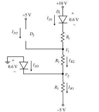
  MICROELECT. CIRCUIT ANALYSIS&DESIGN (LL), Chapter 2, Problem 2.47P , additional homework tip  5

Figure 2

In Figure 2, the Diode D2 is reversed biased. Therefore, the current following through diode D2 is zero.

That is, ID2=0A

Therefore, the current following through diode D2 , ID2 is 0A .

From Figure 2, the voltage at node V2 is,

  V2=0.6V

Apply Kirchhoff’s current law at node V1 .

  V1(0.6)10R1+V1V2R2=0

Substitute 0.6V for V2 , 3kΩ for R1 and 6kΩ for R2 .

  V1(0.6)103k+V1(0.6)6k=0V19.43k+V1+0.66k=02V118.8+V1+0.66=03V118.2=03V1=18.2V1=6.07V

Calculate the current ID1 .

  ID1=100.6V1R1

Substitute 3kΩ for R1 and 6.07V for V1 .

  ID1=100.66.073×103=3.333×103=1.11mA

Therefore, the current following diode D1 , ID1 is 1.11mA .

From Figure 2,

  IR2=ID1=1.11mA

Calculate the current following through resistor, R3 .

  IR3=V2(5)R3

Substitute 2.5kΩ for R3 and 0.6V for V2 .

  IR3=0.6+52.5×103=4.42.5×103=1.76mA

Apply Kirchhoff’s current law at node V2 .

  IR2ID3+IR3=0ID3=IR3IR2

Substitute 1.11mA for IR2 and 1.76mA for IR3

  ID3=1.76mA1.11mA=0.65mA

Therefore, the current following diode D3 , ID3 is 0.65mA .

(d)

Expert Solution
Check Mark
To determine

To find: The values of V1 , V2 and diode current for each.

Answer to Problem 2.47P

The required values are

  ID3 is 0A

  V1 is 4.4V

  V2 is 1.27V

  ID1 is 0.833mA

  ID2 is 0.211mA

Explanation of Solution

Given:

Diode’s cut-in volt- age is Vγ=0.6V
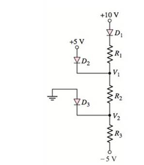
  R1=6kΩ , R2=3kΩ , and R3=6kΩ

  MICROELECT. CIRCUIT ANALYSIS&DESIGN (LL), Chapter 2, Problem 2.47P , additional homework tip  6

Calculation:

Assume diode D3 is OFF and remaining diodes are ON.

Draw the circuit diagram with node voltages and cut-in voltages.
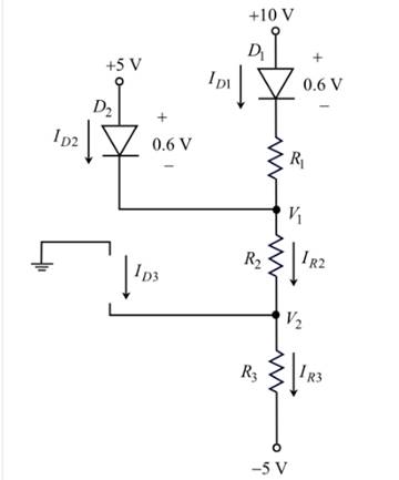
  MICROELECT. CIRCUIT ANALYSIS&DESIGN (LL), Chapter 2, Problem 2.47P , additional homework tip  7

Figure 3

In Figure 3, the Diode D3 is reversed biased. Therefore, the current following through diode D3 is zero.

That is, ID3=0A

Therefore, the current following through diode D3 , ID3 is 0A .

From Figure 1, the voltage at node V1 is,

  V1=50.6=4.4V

Therefore, the node voltage, V1 is 4.4V

Apply Kirchhoff’s current law at node V2 .

  V2(5)R3+V2V1R2=0

Substitute 4.4V for V1 , 3kΩ for R2 and 6kΩ for R3 .

  V2(5)6k+V24.43k=0V2+5+2V28.86k=03V23.8=0V2=1.27V

Calculate the current ID1 .

  ID1=100.6V1R1

Substitute 6kΩ for R1 and 4.4V for V1 .

  ID1=100.64.46×103=56×103=0.833mA

Therefore, the current following diode D1 , ID1 is 0.833mA .

Calculate the current following through resistor, R2 .

  IR2=V1V2R2

Substitute 3kΩ for R2 , 4.4V for V1 and 1.27V for V2 .

  IR2=4.41.273×103=3.133×103=1.044mA

Apply Kirchhoff’s current law at node V1 .

  IR2ID1+ID2=0ID2=IR2ID1

Substitute 0.833mA for ID1 and 1.044mA for IR2 .

  ID2=1.044mA0.833mA=0.211mA

Want to see more full solutions like this?

Subscribe now to access step-by-step solutions to millions of textbook problems written by subject matter experts!
Students have asked these similar questions
Don't use ai to answer I will report you answer
The former expert solved the question, but I didn't understand how he simplified the fractions. A communication satellite is in stationary (synchronous) orbit about the carch (assume altitude of 22.300 statute miles). Its transmitter generates 8.0 W. Assume the transmit- ting antenna is isotropic. Its signal is received by the 210-ft diameter tracking parabo- loidal antenna on the earth at the NASA tracking station at Goldstone, California. Also assume no resistive loss in either antenna, perfect polarization match, and perfect impedance match at both antennas. At a frequency of 2 GHz, determine the: (a) power density (in watts/m²) incident on the receiving antenna. (b) power received by the ground-based antenna whose gain is 60 dB.
Don't use ai to answer I will report you answer

Chapter 2 Solutions

MICROELECT. CIRCUIT ANALYSIS&DESIGN (LL)

Ch. 2 - Consider the circuit shown in Figure 2.19. Let...Ch. 2 - Suppose the currentlimiting resistor in Example...Ch. 2 - Suppose the power supply voltage in the circuit...Ch. 2 - Design a parallelbased clipper that will yield the...Ch. 2 - Sketch the steadystate output voltage for the...Ch. 2 - Consider the circuit in Figure 2.23(a). Let R1=5k...Ch. 2 - Determine the steadystate output voltage O for the...Ch. 2 - Design a parallelbased clipper circuit that will...Ch. 2 - Consider the circuit shown in Figure 2.38, in...Ch. 2 - Consider the circuit shown in Figure 2.39. The...Ch. 2 - Repeat Example 2.11 for the case when R1=8k ,...Ch. 2 - The cutin voltage of each diode in the circuit...Ch. 2 - Prob. 2.12TYUCh. 2 - Consider the OR logic circuit shown in Figure...Ch. 2 - Consider the AND logic circuit shown in Figure...Ch. 2 - (a) Photons with an energy of hv=2eV are incident...Ch. 2 - Determine the value of resistance R required to...Ch. 2 - What characteristic of a diode is used in the...Ch. 2 - Prob. 2RQCh. 2 - Describe a simple fullwave diode rectifier circuit...Ch. 2 - Prob. 4RQCh. 2 - Prob. 5RQCh. 2 - Describe a simple Zener diode voltage reference...Ch. 2 - What effect does the Zener diode resistance have...Ch. 2 - What are the general characteristics of diode...Ch. 2 - Describe a simple diode clipper circuit that...Ch. 2 - Prob. 10RQCh. 2 - What one circuit element, besides a diode, is...Ch. 2 - Prob. 12RQCh. 2 - Describe a diode OR logic circuit. Compare a logic...Ch. 2 - Describe a diode AND logic circuit. Compare a...Ch. 2 - Describe a simple circuit that can be used to turn...Ch. 2 - Consider the circuit shown in Figure P2.1. Let...Ch. 2 - For the circuit shown in Figure P2.1, show that...Ch. 2 - A halfwave rectifier such as shown in Figure...Ch. 2 - Consider the battery charging circuit shown in...Ch. 2 - Figure P2.5 shows a simple fullwave battery...Ch. 2 - The fullwave rectifier circuit shown in Figure...Ch. 2 - The input signal voltage to the fullwave rectifier...Ch. 2 - The output resistance of the fullwave rectifier in...Ch. 2 - Repeat Problem 2.8 for the halfwave rectifier in...Ch. 2 - Consider the halfwave rectifier circuit shown in...Ch. 2 - The parameters of the halfwave rectifier circuit...Ch. 2 - The fullwave rectifier circuit shown in Figure...Ch. 2 - Consider the fullwave rectifier circuit in Figure...Ch. 2 - The circuit in Figure P2.14 is a complementary...Ch. 2 - Prob. 2.15PCh. 2 - A fullwave rectifier is to be designed using the...Ch. 2 - Prob. 2.17PCh. 2 - (a) Sketch o versus time for the circuit in Figure...Ch. 2 - Consider the circuit shown in Figure P2.19. The...Ch. 2 - Consider the Zener diode circuit shown in Figure...Ch. 2 - Consider the Zener diode circuit shown in Figure...Ch. 2 - In the voltage regulator circuit in Figure P2.21,...Ch. 2 - A Zener diode is connected in a voltage regulator...Ch. 2 - Consider the Zener diode circuit in Figure 2.19 in...Ch. 2 - Design a voltage regulator circuit such as shown...Ch. 2 - The percent regulation of the Zener diode...Ch. 2 - A voltage regulator is to have a nominal output...Ch. 2 - Consider the circuit in Figure P2.28. Let V=0 ....Ch. 2 - The secondary voltage in the circuit in Figure...Ch. 2 - The parameters in the circuit shown in Figure...Ch. 2 - Consider the circuit in Figure P2.31. Let V=0 (a)...Ch. 2 - Prob. 2.32PCh. 2 - Each diode cutin voltage is 0.7 V for the circuits...Ch. 2 - The diode in the circuit of Figure P2.34(a) has...Ch. 2 - Consider the circuits shown in Figure P2.35. Each...Ch. 2 - Plot O for each circuit in Figure P2.36 for the...Ch. 2 - Consider the parallel clipper circuit in Figure...Ch. 2 - A car’s radio may be subjected to voltage spikes...Ch. 2 - Sketch the steadystate output voltage O versus...Ch. 2 - Prob. D2.40PCh. 2 - Design a diode clamper to generate a steadystate...Ch. 2 - For the circuit in Figure P2.39(b), let V=0 and...Ch. 2 - Repeat Problem 2.42 for the circuit in Figure...Ch. 2 - The diodes in the circuit in Figure P2.44 have...Ch. 2 - In the circuit in Figure P2.45 the diodes have the...Ch. 2 - The diodes in the circuit in Figure P2.46 have the...Ch. 2 - Consider the circuit shown in Figure P2.47. Assume...Ch. 2 - The diode cutin voltage for each diode in the...Ch. 2 - Consider the circuit in Figure P2.49. Each diode...Ch. 2 - Assume V=0.7V for each diode in the circuit in...Ch. 2 - The cutin voltage of each diode in the circuit...Ch. 2 - Let V=0.7V for each diode in the circuit in Figure...Ch. 2 - For the circuit shown in Figure P2.54, let V=0.7V...Ch. 2 - Assume each diode cutin voltage is V=0.7V for the...Ch. 2 - If V=0.7V for the diode in the circuit in Figure...Ch. 2 - Let V=0.7V for the diode in the circuit in Figure...Ch. 2 - Each diode cutin voltage in the circuit in Figure...Ch. 2 - Let V=0.7V for each diode in the circuit shown in...Ch. 2 - Consider the circuit in Figure P2.61. The output...Ch. 2 - Consider the circuit in Figure P2.62. The output...Ch. 2 - Prob. 2.63PCh. 2 - Consider the circuit shown in Figure P2.64. The...Ch. 2 - The lightemitting diode in the circuit shown in...Ch. 2 - The parameters of D1 and D2 in the circuit shown...Ch. 2 - If the resistor in Example 2.12 is R=2 and the...Ch. 2 - Consider the photodiode circuit shown in Figure...Ch. 2 - Consider the fullwave bridge rectifier circuit....Ch. 2 - Design a simple dc voltage source using a...Ch. 2 - A clipper is to be designed such that O=2.5V for...Ch. 2 - Design a circuit to provide the voltage transfer...
Knowledge Booster
Background pattern image
Electrical Engineering
Learn more about
Need a deep-dive on the concept behind this application? Look no further. Learn more about this topic, electrical-engineering and related others by exploring similar questions and additional content below.
Similar questions
SEE MORE QUESTIONS
Recommended textbooks for you
Text book image
Electric Motor Control
Electrical Engineering
ISBN:9781133702818
Author:Herman
Publisher:CENGAGE L
Three-Phase Half-Wave Rectifier Operation; Author: katkimshow;https://www.youtube.com/watch?v=Uhbr6tbMB9A;License: Standard Youtube License