
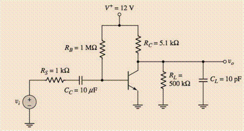
The parameters of the transistor in the circuit in Figure P7.40 are
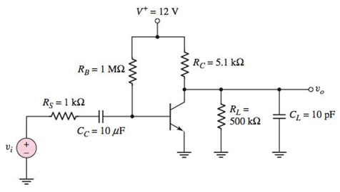 Figure P7.40
a.
To draw: Three equivalent circuits that represent the amplifier in the low frequency range, mid-band range and the high frequency range.
Answer to Problem 7.40P
Three equivalent circuits that represent the amplifier in the low frequency range, mid-band range and the high frequency range are shown in Figure 1, 2 and 3 respectively.
Explanation of Solution
Given:
The diagram is given as:
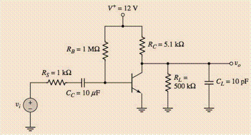
Calculation:
Calculate the value of current
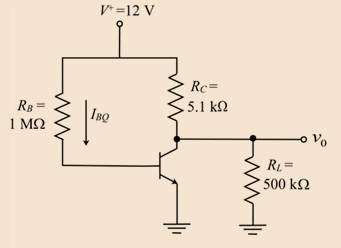
Applying Kirchhoff s voltage law in the above loop:
Here,
Substituting
The quiescent collector current
Here,
Substituting
Evaluating the resistance
Here,
Evaluating the transconductance
Substituting
Figure 2 shows the low −frequency small signal transistor with the output resistance
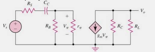
Figure 1
In the mid-frequency range, the coupling and bypass capacitors are short-circuited and the load capacitors are open-circuited.
It shows the mid-frequency small signal transistor with the output resistance

Figure 2
In the high-frequency range, the coupling and bypass capacitors are short-circuited and the load capacitors are included.

Figure 3
Hence, the three equivalent circuits that represent the amplifier in the low-frequency range, mid-band range, and high-frequency range are plotted.
b.
To sketch: The bode magnitude plot.
Answer to Problem 7.40P
The sketch of bode magnitude plot is shown in Figure 4.
Explanation of Solution
Given:
The diagram is given as:
Calculation:
Consider the values, calculated in part (a).
The effect of the coupling capacitor
The figure shows the bode plot for the circuit having a combination of a coupling capacitor and load capacitor:
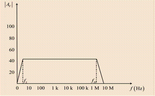
Figure 4
Hence, the bode magnitude plot is sketched.
c.
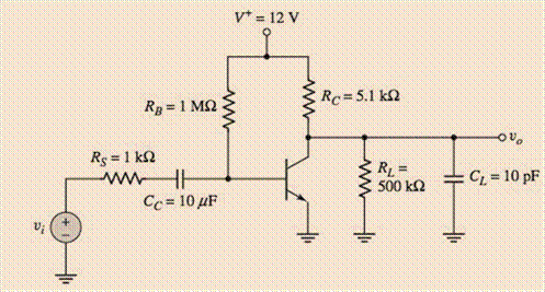
The values of the
Answer to Problem 7.40P
The values are:
Explanation of Solution
Given:
The diagram is given as:
Calculation:
Evaluating the midband gain by short-circuiting the coupling and bypass capacitors and open-circuiting the load capacitors.
Substituting the values,
Evaluating the gain in dB:
Substituting
Hence, the value of gain
Evaluating the equivalent resistance
Substituting
Evaluating the time constant
Substituting
Evaluating the equivalent resistance
Substituting
Evaluating the time constant
Substituting
Evaluate the lower corner frequency
Substituting
Evaluated the upper corner frequency:
Substitute
Want to see more full solutions like this?
Chapter 7 Solutions
MICROELECT. CIRCUIT ANALYSIS&DESIGN (LL)
Additional Engineering Textbook Solutions
Elementary Surveying: An Introduction To Geomatics (15th Edition)
Degarmo's Materials And Processes In Manufacturing
Database Concepts (8th Edition)
Electric Circuits. (11th Edition)
SURVEY OF OPERATING SYSTEMS
Vector Mechanics for Engineers: Statics and Dynamics
- P3. Given the following network, determine: ⚫ 3.a. Equivalent Y ⚫ 3.b. Equivalent A 2 R[2] 10 8 b 20 30 5arrow_forward[Electrical Circuits] P1. Using the mesh current method, calculate the magnitude and direction of: 1.a. I and I (mesh currents) 1.b. I10 (test current in R10 = 1082) 1.c. (Calculate the magnitude and signs of V10) 6[A] 12 [√] بي 10 38 20 4A] Iw -800arrow_forwardNeed handwritten solution do not use chatgptarrow_forward
- [07/01, 16:59] C P: Question: Calculate the following for 100Hz and 500Hz (express all answers in phasor form). Show all work. A) Xc and ZTB) VR1 and VC1 C) IT Handwritten Solution Pleasearrow_forward1. Sketch the root loci of a system with the following characteristic equation: s²+2s+2+K(s+2)=0 2. Sketch the root loci for the following loop transfer function: KG(s)H(s)=- K(s+1) s(s+2)(s²+2s+4)arrow_forward3. For the unity feedback system with forward path transfer function, G(s), below: G(s)= K(s² +8) (s+4)(s+5) Sketch the root locus and show the breakaway/break-in point(s) and jo-axis crossing. Determine the angle of arrival and K value at the breakaway/break- in point(s). Give your comment the system is stable or unstable.arrow_forward
- Find the step response of each of the transfer functions shown in Eqs. (4.62) through (4.64) and compare them. [Shown in the image]Book: Norman S. Nise - Control Systems Engineering, 6th EditionTopic: Chapter-4: Time Response, Example 4.8Solve the math with proper explanation. Please don't give AI response. Asking for a expert verified answer.arrow_forward2. With respect to the circuit shown in Figure 2 below V2 -R1 R2 R4 w R3 R5 Figure 2: DC Circuit 2 a. Using Ohm's and Kirchhoff's laws calculate the current flowing through R3 and so determine wattage rating of R3. b. Verify your results with simulations. Note: you must use the values for the components in Table 2. Table 2 V2 (Volts) R1 (KQ) R2 (KQ) R3 (KQ) R4 (KQ) R5 (KQ) 9 3.3 5 10 6 1 3.3arrow_forwardDon't use ai to answer i will report your answerarrow_forward
- Don't use ai to answer I will report you answerarrow_forwardcircuit value of i1 and i2arrow_forwardIn the circuit shown in the figure, the switch opens at time t = 0. For t≥ 0 use I(t) and V₁(t) or Find Vc(t) and lc(t). D to icht) w 43 ViLC+) + vc(+) 5. F + 1252 18 A 3) 2H2VLCH 8 V 4л warrow_forward
 Introductory Circuit Analysis (13th Edition)Electrical EngineeringISBN:9780133923605Author:Robert L. BoylestadPublisher:PEARSON
 Delmar's Standard Textbook Of ElectricityElectrical EngineeringISBN:9781337900348Author:Stephen L. HermanPublisher:Cengage Learning
 Programmable Logic ControllersElectrical EngineeringISBN:9780073373843Author:Frank D. PetruzellaPublisher:McGraw-Hill Education
 Fundamentals of Electric CircuitsElectrical EngineeringISBN:9780078028229Author:Charles K Alexander, Matthew SadikuPublisher:McGraw-Hill Education
 Electric Circuits. (11th Edition)Electrical EngineeringISBN:9780134746968Author:James W. Nilsson, Susan RiedelPublisher:PEARSON
 Engineering ElectromagneticsElectrical EngineeringISBN:9780078028151Author:Hayt, William H. (william Hart), Jr, BUCK, John A.Publisher:Mcgraw-hill Education,


