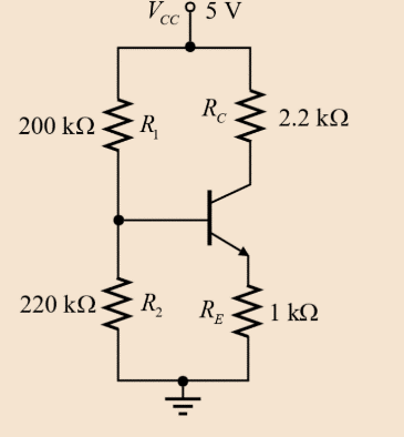
For the circuit in Figure 7.41(a), the parameters are,
(i)
a.
The midband current gain.
Answer to Problem 7.10EP
The value of mid-band current gain
Explanation of Solution
Given:
The parameters for the given circuit:
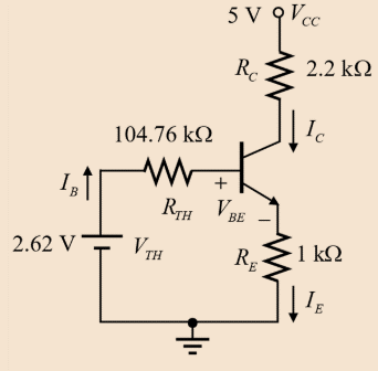
Drawing the DC equivalent circuit for the given circuit:

Evaluating the Thevenin equivalent voltage at the base terminal:
Evaluating the Thevenin equivalent resistance at the base terminal:
Drawing the DC equivalent circuit as shown below:

Evaluating the value of base current
Evaluating the value of collector current
Evaluating the value of small signal parameters
Evaluating the value of small signal parameters
Drawing the small-signal equivalent circuit for the mid band current gain:

Applying the nodal analysis at the node
Applying the current division rule at the output node:
Evaluating the value of mid band current gain
Hence, the value of mid-band current gain
b.
The Miller capacitance CM for the given values of the
Answer to Problem 7.10EP
The Miller capacitances for the both cases are:
Explanation of Solution
Given:
The parameters for the given circuit:
The value of the capacitances are given as:
( i ) The value of capacitance
Evaluating the value of Miller capacitance for
Hence, the value of Miller capacitance for
(ii)
The value of capacitance:
Evaluating the value of Miller capacitance for
Hence, the value of the Miller capacitance for
c.
The upper 3-dB frequency for the given values of the
Answer to Problem 7.10EP
The 3-dB frequencies for the both cases are:
Explanation of Solution
Given:
The parameters for the given circuit:
The value of the capacitances are given as:
(i)
The value of Miller capacitance for
Since,
Evaluating the upper
Hence, the upper
(ii)
The value of Miller capacitance for
Since,
Evaluating the upper
Hence, the upper
Want to see more full solutions like this?
Chapter 7 Solutions
MICROELECT. CIRCUIT ANALYSIS&DESIGN (LL)
- DU 1. Describe the operations of Q1, Q2 and LM566. 2. Describe the functions of VR1 and VR2. R6 lk R3 BRUD 3. If the input frequency is higher than the FSK frequency, does the FSK modulator operate normally? 0+12V R10 5.6k 6 10k VRI 500k U₁ LM566 3 VCO output 7 Digital input R₁ VR2 10k ww 1k Qi C945 C945 C5 I 0.1 uF C6 luF C₁ 0.01μ R2 10k ww R$ 100k C3 +12V 0.01μ R9 100k +12V 6 R710k Rs 100k 6 R4 100k P FSK output ww ww + www + 3 3 4 U U₂ 1000p -12V HA741 1000p-12V µА741 Fig. 13-2 FSK modulator CTS circuit.arrow_forward. 30-dB, right-circularly polarized antenna in a radio link radiates 5-W of power t 2 GHz. The input impedance of this antenna is 75 ohms, and it is attached ɔ a 50-ohm transmission line. The receiving antenna has an impedance mismatch at its terminals, - which leads to a VSWR of 2. The receiving antenna is about 95% efficient and has a field pattern near the beam maximum given by E, = (2âx + jây) F, (0, 0). The distance between the two antennas is 4,000 km, and the receiving antenna Directivity is 100. Determine the Minimum power Delivered to receiving antenna. 1arrow_forwardOpen plc - ladder logic To control traffic, we have red lights to stop cars and green lights to initiate entry/exit. If a car is in the lane, then the red lights turn ON. If no cars are in the lane, then the green lights turn ON. Upon turning ON the main switch button, the main switch indicator should turn ON and the system should start with green lights ON and red lights OFF?arrow_forward
- 3-4) 3.4-2 Signals g₁(t) = 104П(104) and g2(t) = 8(t) are applied at the inputs of the ideal low-pass filters H₁(f)=(f/20,000) and H2(f) = П(f/10,000) (Fig. P3.4-2). The outputs y₁ (t) and y2(t) of these filters are multiplied to obtain the signal y(t) = y1 (1)y2(t). (a) Sketch G1(f) and G2(f). (b) Sketch H₁(f) and H₂(f). (c) Sketch Y₁ (f) and Y2(f). (d) Find the bandwidths of y₁ (t), y2(t), and y(t). 8₁ (1) H₁(f) y, (t) y(t) = y₁ (1) y2 (1) 82(1) ½⁄2 (1) H₂(f)arrow_forwardsolve the differential equation y'' -2y'-3y=x³e^5x cos(3x) Don't use AI,I need it handwrittenarrow_forward3-3) Similar to Lathi & Ding prob. 3.3-7. The signals in the figure below are modulated signals with carrier cos(5t). Find the Fourier transforms of these signals using the appropriate properties of the Fourier transform and text Table 3.1. The sketch the magnitude and phase spectra for figure parts (a) and (b). Hint: these functions can be expressed in the form g(t) cos(2лfot) (a) 1 1 2π www. σπ (b) (c) όπarrow_forward
- 3-1) Similar to Lathi & Ding prob. 3.1-1. Use direct integration to find the Fourier transforms of the signals shown below. a) g₁(t) = II(t − 2) + 2 exp (−3|t|) b) g(t) = d(t+2)+3e¯u (t − 2)arrow_forward3-2) Lathi & Ding prob. 3.1-5. From the definition in eq. 3.1b, find the inverse Fourier transforms of the spectra in the figure below. G(f) COS лf 10 (a) G(f) 1 -B B (b)arrow_forwardFundamentals of Energy Systems HW 4 Q2arrow_forward
 Introductory Circuit Analysis (13th Edition)Electrical EngineeringISBN:9780133923605Author:Robert L. BoylestadPublisher:PEARSON
 Delmar's Standard Textbook Of ElectricityElectrical EngineeringISBN:9781337900348Author:Stephen L. HermanPublisher:Cengage Learning
 Programmable Logic ControllersElectrical EngineeringISBN:9780073373843Author:Frank D. PetruzellaPublisher:McGraw-Hill Education
 Fundamentals of Electric CircuitsElectrical EngineeringISBN:9780078028229Author:Charles K Alexander, Matthew SadikuPublisher:McGraw-Hill Education
 Electric Circuits. (11th Edition)Electrical EngineeringISBN:9780134746968Author:James W. Nilsson, Susan RiedelPublisher:PEARSON
 Engineering ElectromagneticsElectrical EngineeringISBN:9780078028151Author:Hayt, William H. (william Hart), Jr, BUCK, John A.Publisher:Mcgraw-hill Education,


