
Videos
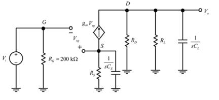
In the common−source amplifier in Figure 7.25(a) in the text, a source bypass capacitor is to be added between the source terminal and ground potential. The circuit parameters are
a.
To derive: The small signal voltage gain expression.
Answer to Problem 7.41P
The expression for small signal voltage gain:
Explanation of Solution
Given:
The circuit parameter is given as:
The transistor parameter are given as:
Drawing the small signal model of the circuit with the source bypass capacitor:
Applying the Ohm’s law to the drain terminal:
Evaluating the input voltage
Evaluating the ratio of output voltage to the input voltage:
Therefore, the expression for small signal voltage gain:
b.
The expression for the time constant associated with the upper 3dB frequency.
Answer to Problem 7.41P
The expression for the time constant associated with the upper 3 Db frequency is:
Explanation of Solution
Given:
The circuit parameter is given as:
The transistor parameter are given as:
The expression for time constant
Here, the expression for the time constant associated with the upper 3 Db frequency is:
c.
The time constant, upper 3 dB frequency and the small signal midband voltage gain.
Answer to Problem 7.41P
The small signal mid-band voltage gain is -4.7.
Explanation of Solution
Given:
The circuit parameter is given as:
The transistor parameter are given as:
The equation for the time constant is given as:
Substituting the known values in the above equation:
Hence, the value of time constant,
Now, evaluating the upper
Substitute
Hence, the value of upper
Applying the Kirchhoff s voltage law to the outer loop:
Substituting the known values:
Evaluating the value of current
Substituting the known values:
Evaluating the transconductance
Substituting the known values in the above equation:
Since, the voltage gain is given as:
Evaluating the mid-band voltage gain
Substituting the known values in the above equation:
Hence, the small signal mid-band voltage gain is -4.7.
Want to see more full solutions like this?
Chapter 7 Solutions
MICROELECT. CIRCUIT ANALYSIS&DESIGN (LL)


- Question 5 The following data were obtained from testing a 48-kVA 240/4800 V step up transformer. Open-circuit test Short-circuit test Voltage (V) 240 150 Current (I) 2 10 Power (W) 120 600 Determine the equivalent circuit of the transformer as viewed from the primary side. Ans: Rc = 480 ohm, Xm = 123.94 ohm, Reqp = 0.015 ohm, Xeqp = 0.034 ohmarrow_forwardFrom the following mass-spring system, obtain its transfer function and pole-zero wwwwwwww wwww diagram in MATLAB. Analyze how stability varies when entering values. wwwww (4)x1 ▷ x(t) M f(t) B f(t) is the input variable and x(t) is the controlled variable.arrow_forwardR2 L3 C5 BRF_OUT HH Sine_OUT 100 1m 100n C3 C4 100n 100n Figure 9. Square to sine waveform converter circuit How do we make sense of this? First, we note that R2 and C3 form a first order low pass filter and L3 and C4 form another low pass filter. Both low pass filters have been set at the same cutoff frequency. The combination of both form a two stage filter to remove the high frequency content present in the DAB signal. Capacitor C5 is used to remove any residual DC offset in the signal. But let's just deal with the AC steady state response, which means that you don't need to know any of these details, and then can conveniently treat this circuit as a blackbox. What is the theoretical cutoff frequency for the RC and LC filters shown in Figure 9? Answer to within 1% accuracy. (a) RC Filter cutoff frequency (f 1) = kHzarrow_forward
- For the following steady-state AC circuit, find the complex output voltage, VO, shown in the diagram. Write the answer in polar form (angles in degrees), accurate within 1%. L1=0.7H, L2=5H, C=14F, R=0.60, and w=0.7 rad/s L1 m Vo R Vs 5/30°V Answer: ய ww L2 23arrow_forwardPlease draw logic circuitarrow_forwardA 220-volt, 20-horsepower compound motor (long shunt, Figure 21–16A) has an armature resistance of 0.25 ohm, series field resistance of 0.19 ohm, and shunt field resistance of 33 ohms. a. Calculate the current taken by the motor at the instant of starting if it is con-nected directly to the 220-volt line. b. Calculate the current when the motor is running if the armature is developing 184 volts counter-emf.arrow_forward
- Design a modulo-11 ripple (asynchronous) up-counter with negative edge-triggered T flip-flops and draw the corresponding logic circuit. (I)Build the state diagram and extract the state table (II)Draw the logic circuit (III)What is the maximum modulus of the counter?arrow_forwardthe diagram show 4 motor connected to a k-35 controller. I would like detail explanation to know how the circuit work. Is the controller compatible with the motor? The motor shown is series, parallel or both?arrow_forwardplease draw logic diagram pleasearrow_forward
- Please draw the diagrams please thank youarrow_forwardA plane wave propagating through a medium with &,,-8 μr = 2 has: E = 0.5 e-j0.33z sin (108 t - ẞz) ax V/m. Determine (a) ẞ (b) The loss tangent (c) Wave impedance (d) Wave velocity (e) H fieldarrow_forward2) The phase voltage at the terminals of a balanced three-phase Y-connected load is 2400 V. The load has an impedance of 16+j12 2/6 and is fed from a line having an impedance of 0.10+j0.80 2/6. The Y- connected source at the sending end of the line has a positive phase sequence and an internal impedance of 0.02+j0.16 2/6. Use the a-phase voltage at the load as the reference. a) Construct the a-phase equivalent circuit of the system b) Calculate the line currents IaA, IbB, and Icc c) Calculate the phase voltages at the terminals of the source, Van, Vbn, Vcn- d) Calculate the line voltages at the source, Vab, Vbc and Vca. e) Calculate the internal phase-to-neutral voltages at the source, Va'n, Vb'n, Ve'n,arrow_forward
 Introductory Circuit Analysis (13th Edition)Electrical EngineeringISBN:9780133923605Author:Robert L. BoylestadPublisher:PEARSON
 Delmar's Standard Textbook Of ElectricityElectrical EngineeringISBN:9781337900348Author:Stephen L. HermanPublisher:Cengage Learning
 Programmable Logic ControllersElectrical EngineeringISBN:9780073373843Author:Frank D. PetruzellaPublisher:McGraw-Hill Education
 Fundamentals of Electric CircuitsElectrical EngineeringISBN:9780078028229Author:Charles K Alexander, Matthew SadikuPublisher:McGraw-Hill Education
 Electric Circuits. (11th Edition)Electrical EngineeringISBN:9780134746968Author:James W. Nilsson, Susan RiedelPublisher:PEARSON
 Engineering ElectromagneticsElectrical EngineeringISBN:9780078028151Author:Hayt, William H. (william Hart), Jr, BUCK, John A.Publisher:Mcgraw-hill Education,