
Videos
Figure P7.62 shows the high−frequency equivalent circuit of an FET, including a source resistance
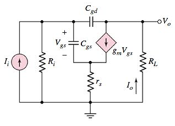
Figure P7.62
Want to see the full answer?
Check out a sample textbook solution
Chapter 7 Solutions
MICROELECT. CIRCUIT ANALYSIS&DESIGN (LL)


- c) An RC circuit is given in Figure Q1. vi(t) and vo (t) are the input and output voltages. (i) Derive the transfer function of the circuit. (ii) With a unit step change vi(t) applied to the circuit, derive and sketch the time response of the circuit. R₁ R2 v₁(t) R3 C₁ v₁(t) R₁ = R₂ = 10 k R3 = 100 kn C₁ = 100 μF Figure Q1. RC circuit.arrow_forwardc) A RC circuit is given in Figure Q1.1. Vi(t) and Vo(t) are the input and output voltages. (i) Derive the transfer function of the circuit. (ii) With a unit step change of Vi(t) applied to the circuit, derive the time response of the circuit. C₁ C₂ Vi(t) Vo(1) R₁ C₂ R-25 k C=C2=50 µF Figure Q1.1. RC circuit.arrow_forwardAnswer 2 questions for 100 marks Question 1: Process Design [25 marks] An incomplete process design of a flash drum distillation unit is presented in Figure 1. The key variables to be controlled are flow rate, temperature, composition, pressure and liquid level in the drum. Disturbances are observed in the feed temperature and composition. Heat exchangers Drum Vapor Liquid Pump Figure 1: Incomplete process design of a distillation unit Answer the following questions briefly and in a qualitative fashion: a) Determine which sensors and final elements are required so that the important variables can be controlled. Sketch them in the figure using correct instrumentation tags. Describe briefly what instruments you will use and where they should be located. Reflect on the potential presence of a flow controller upstream of your process design (not shown in the diagram). How would this affect the level controller in the drum? b) [10 marks] Describe briefly how you qualitatively determine the…arrow_forward
- Answer 2 questions for 100 marks Question 1: Process Design [25 marks] An incomplete process design of a flash drum distillation unit is presented in Figure 1. The key variables to be controlled are flow rate, temperature, composition, pressure and liquid level in the drum. Disturbances are observed in the feed temperature and composition. Heat exchangers Drum Vapor Liquid Pump Figure 1: Incomplete process design of a distillation unit Answer the following questions briefly and in a qualitative fashion: a) Determine which sensors and final elements are required so that the important variables can be controlled. Sketch them in the figure using correct instrumentation tags. Describe briefly what instruments you will use and where they should be located. Reflect on the potential presence of a flow controller upstream of your process design (not shown in the diagram). How would this affect the level controller in the drum? b) [10 marks] Describe briefly how you qualitatively determine the…arrow_forwardQuestion 2: Process Control [75 marks] As a process engineer, you are tasked to control the process shown in Figure 2. For biomedical engineers, the process could be interpreted as the injection of a solution of a medication compound A, with initial concentration CAO, into a human body, simplified as a Continuously Stirred Tank Reactor (CSTR). Therefore, your task is to analyse and model this process. The equipment consists of a mixing tank, mixing pipe and CSTR. F₁ Сло CA2 V₁ mixing pipe F4 CA4 F3 CA3 mixing tank Fs CAS Vs stirred-tank reactor Figure 2: Mixing and reaction processes Assumptions used for modelling are as follows: I. Both tanks are well mixed and have constant volume and temperature. II. All pipes are short and contribute negligible transportation delay, III. All flow rates are constant. All densities are constant and uniform throughout. IV. The first tank is a mixing tank. V. VI. The mixing pipe has no accumulation, and the concentration CA3 is constant The second tank…arrow_forwarda) Reflect on the assumptions and briefly explain their implications for your model. Do you agree with the assumptions? If not, briefly suggest improved assumptions. [6 marks] b) Derive a linear(ised) model (algebraic or differential equation) relating C'A2(t) to C'Ao(f). How do you define your system? What type of balance do you need to solve for this purpose? [12 marks] c) Derive a linear(ised) model (algebraic or differential equation) relating C'A4(t) to C'A2(f). Show your balance equation. [12 marks] d) Derive a linear(ised) model (algebraic or differential equation) relating C'A5(t) to C'A4(f). Show your balance equation. [12 marks] e) Combine the models in parts (a) to (c) into one equation relating C'A5 to C'Ao using Laplace transforms. [15 marks] f) Is the response (for example to step input) stable or unstable? Is the response periodic? Is the response damped? [6 marks] g) Carry out an inverse Laplace Transform for C'Ao(s) = A CAO/s (step function) to find C'A5(t) in the time…arrow_forward
- I need helparrow_forwardThe values of the circuit elements in the circuit shown in the figure are given below.The initial energies of the capacitors and the coil are zero.Accordingly, how many volts is the voltage vo at t=0.55 seconds? vs(t) = 2cos(4000t)u(t) VR = 19 ohmL = 20 HC1 = 1/5 FC2 = 1/2 Farrow_forwardcould you please show steps on how the answer was derived. Vo(t)=3.922 cos(1000t-71.31')Varrow_forward
- can you show the steps to answer question.arrow_forwardQ2. Figure Q2 shows a block diagram with an input of C(s) and an output R(s). a) C(s) K₁ R(s) K2 1 + 5s 1+2s Figure Q2. Block diagram of control system. Simply the block diagram to get the transfer function of the system C(s)/R(s). b) What is the order of the system? c) What is the gain of the system? d) Determine the values of K₁ and K₂ to obtain a natural frequency w of 0.5 rad/s and damping ratio of 0.4. e) What is the rise time and overshoot of the system with a unit step input?arrow_forwardQ4. a) A purely derivative controller (i.e. with a zero at the origin only) is defined by an improper transfer function. Considering its asymptotic behaviour, explain why a purely derivative controller is difficult to implement in practice. Relate your explanation to the potential limitations on system performance. b) Discuss the potential issues faced by a control system with a large cut-off frequency. Relate your discussion to the implications on system performance. c) The transfer function of a lag compensator is given by 2 KPID(S) = 2.2++0.2s S By using the asymptotic approximation technique: (i) Obtain the standard form and corner frequency for each individual component of KPID(S). (ii) Clearly describe the asymptotic behaviour of each individual component of KPID(S).arrow_forward
 Introductory Circuit Analysis (13th Edition)Electrical EngineeringISBN:9780133923605Author:Robert L. BoylestadPublisher:PEARSON
 Delmar's Standard Textbook Of ElectricityElectrical EngineeringISBN:9781337900348Author:Stephen L. HermanPublisher:Cengage Learning
 Programmable Logic ControllersElectrical EngineeringISBN:9780073373843Author:Frank D. PetruzellaPublisher:McGraw-Hill Education
 Fundamentals of Electric CircuitsElectrical EngineeringISBN:9780078028229Author:Charles K Alexander, Matthew SadikuPublisher:McGraw-Hill Education
 Electric Circuits. (11th Edition)Electrical EngineeringISBN:9780134746968Author:James W. Nilsson, Susan RiedelPublisher:PEARSON
 Engineering ElectromagneticsElectrical EngineeringISBN:9780078028151Author:Hayt, William H. (william Hart), Jr, BUCK, John A.Publisher:Mcgraw-hill Education,