
Introductory Circuit Analysis (13th Edition)
13th Edition
ISBN: 9780133923605
Author: Robert L. Boylestad
Publisher: PEARSON
expand_more
expand_more
format_list_bulleted
Concept explainers
Videos
Textbook Question
Chapter 8, Problem 3P
Find voltage
(with polarity) across the ideal current source in Fig. 8.105.
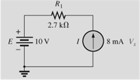 Fig. 8.1ss05
Expert Solution & Answer

Learn your wayIncludes step-by-step video

schedule02:18
Students have asked these similar questions
Please show all steps
A plane wave propagating in the +z direction in medium 1 is normally incident to medium 2 located at
the z=0 plane as below. Both mediums are general, characterized by ( ε i, Mi, Ơi ).
tot
=
[ ει μη σ]
[ε, μη σε ]
Ex
Ex
tot
E₁₂ (z) = Ee
Ex
z=0
From conservation of energy: P₁AV'(z=0) + Piav'(z=0) = P2av²(z=0).
Using the above show for lossless media that: ( 1 - ||²) = (1/M2 )|T|² .
A plane wave propagating in the +z direction in medium 1 is normally incident to medium 2 located at
the z=0 plane as below. Both mediums are general, characterized by ( ε i, Hi, σ¡ ).
[ ει μη σ]
Ex
[ ει μη ση ]
Ex
tot
E₁₂ (z) = E'₁e¹²
-122
E(z) = Ee+ E₁₁₁²
E₁x
z=0
1. Specify the electric field reflection coefficient г and transmission coefficient T:
E
ΓΔ
E
E
TA
EL
2. Show that T=1+г. Can the transmitted electric field amplitude in region 2 be LARGER than the
incident electric field amplitude?
3. Determine expressions for P₁AV'(z), PIAV'(z) and P2AV'(z) (note the sign for the reflected power
direction should be (-z).
Chapter 8 Solutions
Introductory Circuit Analysis (13th Edition)
Ch. 8 - For the network of Fig. 8.103: a. Find the...Ch. 8 - For the network of Fig. 8.104: a. Determine the...Ch. 8 - Find voltage Vs (with polarity) across the ideal...Ch. 8 - For the network in Fig. 8.106: a. Find voltage Vs....Ch. 8 - Find the voltage V3 and the current I2 for the...Ch. 8 - For the network in Fig. 8.108: a. Find the...Ch. 8 - Convert the voltage sources in Fig. 8.109 to...Ch. 8 - Convert the current sources in Fig. 8.110 to...Ch. 8 - For the network in Fig. 8.111: Find the current IL...Ch. 8 - For the configuration of Fig. 8.112: a. Convert...
Ch. 8 - For the network in Fig. 8.113: a. Replace all the...Ch. 8 - Find the voltage Vs and the current I1 for the...Ch. 8 - Convert the voltage sources in Fig. 8.115 to...Ch. 8 - For the network in Fig. 8.116, reduce the network...Ch. 8 - Using branch-current analysis, find the magnitude...Ch. 8 - For the network of Fig. 8.118: Determine the...Ch. 8 - Using branch-current analysis, find the current...Ch. 8 - Using branch-current analysis, find the current...Ch. 8 - For the network in Fig. 8.121: a. Write the...Ch. 8 - Using the general approach to mesh analysis,...Ch. 8 - Using the general approach to mesh analysis,...Ch. 8 - Using the general approach to mesh analysis,...Ch. 8 - Using the general approach to mesh analysis,...Ch. 8 - Determine the mesh currents for the network of...Ch. 8 - Write the mesh equations for the network of Fig....Ch. 8 - Write the mesh equations for thesss network of...Ch. 8 - Write the mesh currents for the network of Fig....Ch. 8 - Redraw the network of Fig. 8.125 in a manner that...Ch. 8 - For the transistor configuration in Fig. 8.126: a....Ch. 8 - Using the supermesh approach, find the current...Ch. 8 - Using the supermesh approach, find the current...Ch. 8 - Using the format approach to mesh analysis, write...Ch. 8 - Using the format approach to mesh analysis, write...Ch. 8 - Using the format approach to mesh analysis, write...Ch. 8 - Write the mesh equations for the network of Fig....Ch. 8 - Write the mesh equations for the network of Fig....Ch. 8 - a. Write the mesh equations for the network of...Ch. 8 - Write the mesh equations for the network of Fig....Ch. 8 - Write the mesh equations for the network of Fig....Ch. 8 - a. Write the mesh equations for the network of...Ch. 8 - a. Write the nodal equations using the general...Ch. 8 - Write the nodal equations using the general...Ch. 8 - a. Write the nodal equations using the general...Ch. 8 - a. Write the nodal equations for the network of...Ch. 8 - a. Write the nodal equations for the network of...Ch. 8 - a. Write the nodal equations for the network of...Ch. 8 - Write the nodal equations for the network of Fig....Ch. 8 - Write the nodal equations for the network of Fig....Ch. 8 - Write the nodal equations for the network of Fig....Ch. 8 - Using the supernode approach, determine the nodal...Ch. 8 - Using the supernode approach, determine the nodel...Ch. 8 - Determine the nodal voltages of Fig. 8.130 using...Ch. 8 - Convert the voltage source of Fig 8.131 to a...Ch. 8 - Convert the voltage source of Fig. 8.136 to a...Ch. 8 - Apply the format approach of nodal analysis to the...Ch. 8 - Using the format approach, find the nodal voltages...Ch. 8 - Convert the voltage sources of Fig. 8.129 to...Ch. 8 - For the network of Fig. 8.135: a. Convert the...Ch. 8 - For the bridge network in Fig. 8.141: a. Write the...Ch. 8 - For the network in Fig. 8.141: a. Write the nodal...Ch. 8 - For the bridge in Fig. 8.142: a. Write the mesh...Ch. 8 - For the bridge network in Fig. 8.142: a. Write the...Ch. 8 - Determine the current through the source resistor...Ch. 8 - Repeat Problem 63 for the network of Fig. 8.144....Ch. 8 - Using a -Y or Y- conversion, find the current I...Ch. 8 - Convert the of 6.8 k resistors in Fig. 8.146 to...Ch. 8 - For the network of Fig. 8.147, find the current I...Ch. 8 - a. Using a -Y or Y- conversion, find the current...Ch. 8 - The network of Fig. 8.149 is very similar to the...Ch. 8 - a. Replace the TT configuration in Fig.8.150...Ch. 8 - Using Y or Yconversion, determine the total...Ch. 8 - Using schematics, find the current through each...Ch. 8 - Using schematics, find the mesh currents for the...Ch. 8 - Using schematics, determine the nodal voltages for...
Additional Engineering Textbook Solutions
Find more solutions based on key concepts
7.13* For a bearing
DE = NUS 5 53’56 ”WT and angles to the right, compute the bearing of PG if angle
DEF 2 88°...
Elementary Surveying: An Introduction To Geomatics (15th Edition)
Repeat Exercise 2 in Chapter 7, but use an instance of ArrayList instead of an array. Do not read the number of...
Java: An Introduction to Problem Solving and Programming (8th Edition)
Use the following tables for your answers to questions 3.7 through 3.51 : PET_OWNER (OwnerID, OwnerLasst Name, ...
Database Concepts (8th Edition)
Look at the following pseudocode. If it were a real program, what would it display? Declare Integer number1 = 1...
Starting Out with Programming Logic and Design (5th Edition) (What's New in Computer Science)
What is the difference between a formal programming language and a pseudocode?
Computer Science: An Overview (13th Edition) (What's New in Computer Science)
Create a flowchart that shows the necessary steps for making the cookies in the following recipe: Ingredients: ...
Starting Out With Visual Basic (8th Edition)
Knowledge Booster


Learn more about
Need a deep-dive on the concept behind this application? Look no further. Learn more about this topic, electrical-engineering and related others by exploring similar questions and additional content below.Similar questions
- 2) In the ideal transformer circuit shown below find Vo and the complex power supplied by the source. 292 www b 1:4 16 Ω ww + + 240/0° V rms -12492arrow_forward3) In the ideal autotransformer circuit shown below find 11, 12 and lo. Find the average power delivered to the load. (hint: write KVL for both sides) 20/30° V(+ 2-1602 200 turns V₂ 10 + j40 Ω 80 turns V₁arrow_forward1) Find Vo in the following circuit. Assume the mesh currents are clockwise. ΠΩ Ω ΖΩ ww 1Ω ww 24/0° (± 6 Ω j4 Ω 1Ω +arrow_forward
- Please show all stepsarrow_forward11-3) similar to Lathi & Ding, Prob. P.6.8-1 Consider the carrier modulator shown in the figure below, which transmits a binary carrier signal. The baseband generator uses polar NRZ signaling with rectangular pulses. The data rate is 8 Mbit/s. (a) If the modulator generates a binary PSK signal, what is the bandwidth of the modulated output? (b) If the modulator generates FSK with the difference fel - fco = 6 MHz (cf. Fig 6.32c), determine the modulated signal bandwidth. Binary data source Baseband signal generator Modulated output Modulator N-E---arrow_forwardSolve this problem and show all of the workarrow_forward
- Q3: Why is the DRAM cell design simpler but slower than SRAM?arrow_forward5052 ми a JXL 000 +2 16s (wt) bi jxc M 100♫ ZL. Find the Value of XL & X c if the Circuit trans for Max. Power to (ZL).arrow_forwardChoose the best answer for each: 1. What does SRAM use to store data? 。 a) Capacitors ob) Latches 。 c) Flip-flops od) Transistors 2. Which RAM type requires refreshing? o a) SRAM ob) DRAM 。 c) ROM od) Flash 3. What type of memory retains data only while power is on? a) ROM 。 b) EEPROM o c) DRAM od) Flash 4. How many addresses can a 15-bit address bus handle? o a) 32k • b) 64k o c) 16k od) lk 5. What operation occurs when data is copied out of memory without erasing? oa) Write ob) Read o c) Refresh o d) Load 6. DRAM cells store bits using: a) Flip-flops 。 b) Capacitors c) Diodes od) Resistors 7. The cache located inside the CPU is: 。 a) L2 cache o b) LI cache °c) ROM od) HDD 8. SDRAM is synchronized with: o a) Cache ob) Data Bus c) System Clock od) Hard Disk 9. The bus that carries commands is called: o a) Data Bus b) Control Bus o c) Address Bus o d) Logic Bus 10. What is the main use of SRAM? o Disk storage o Cache o Main memory o Registers 11. The smallest addressable unit in…arrow_forward
- Q4: A cache memory is 128k × 16. How many bytes can it store?arrow_forwardSketch the output of the analogue computer shown below and find its closest describing function [suppose any variable to find the DF] +1 ew2 HI e2 1.0 +21 LO SJ eo SJ ew LO 1.0 +|e1| HI -1 ew1 ek(1 + e。) |e1| k = 1+|e1| Figure V-5 Feedback Limiter Behavior ROUNDED, DUE TO DIODE NONLINEARITY LIMIT VOLTAGE 409 DIODE CONDUCTS First, write the output transaction, then draw the output wave, and then find the Describing function. I need to solve the question step by step, with an explanation of each step.arrow_forwardSketch the output of the analogue computer shown below and find its closest describing function [suppose any variable to find the DF] SJ ew2 ew₁ HI |e2| 2 LO 1.0 +21 LO -1 HI Jel 1.0+|e1| ROUNDED, DUE TO DODE NONLINEARITY LIMIT VOLTAGE DIODE CONDUCTS ew1e, -k(1+ e。) k = |e1| 1+|e1| Figure 1-5 Feedback Limiter Behavior First, write the output transaction, then draw the output wave, and then find the Describing function. I need to solve the question step by step, with an explanation of each step.arrow_forward
arrow_back_ios
SEE MORE QUESTIONS
arrow_forward_ios
Recommended textbooks for you
 Delmar's Standard Textbook Of ElectricityElectrical EngineeringISBN:9781337900348Author:Stephen L. HermanPublisher:Cengage Learning
Delmar's Standard Textbook Of Electricity
Electrical Engineering
ISBN:9781337900348
Author:Stephen L. Herman
Publisher:Cengage Learning
Kirchhoff's Rules of Electrical Circuits; Author: Flipping Physics;https://www.youtube.com/watch?v=d0O-KUKP4nM;License: Standard YouTube License, CC-BY