Concept explainers
Videos
For the network in Fig. 8.121:
a. Write the equations necessary to solve for the branch currents.
b. By substitution of Kirchhoff’s current law, reduce the set to three equations.
c. Rewrite the equations in a format that can be solved using third-order determinants.
d. Solve for the branch current through the resistor
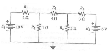
Fig. 8.121
Want to see the full answer?
Check out a sample textbook solution
Chapter 8 Solutions
Introductory Circuit Analysis (13th Edition)
Additional Engineering Textbook Solutions
Thermodynamics: An Engineering Approach
Vector Mechanics For Engineers
Vector Mechanics for Engineers: Statics and Dynamics
Fluid Mechanics: Fundamentals and Applications
Elementary Surveying: An Introduction To Geomatics (15th Edition)
Starting Out with Programming Logic and Design (5th Edition) (What's New in Computer Science)


- I have uploaded the rules, please explain step by step and which rule you have appliedarrow_forwardUsing the CCS Compiler method to solve this question Write a PIC16F877A program that flash ON the 8-LED's connected to port-B by using two switches connected to port-D (Do & D₁) as shown in figure below, according to the following scenarios: (Hint: Use 500ms delay for each case with 4MHz frequency) 1. When Do=1 then B₁,B3,B7 are ON. 2. When Do 0 then Bo,B2, B4, B5, B6 are ON. 3. When D₁=1 then B4,B,,B6,B7 are ON. 4. When D₁-0 then Bo,B1,B2,B3 are ON.arrow_forwardUse the ramp generator circuit in Fig. B2a to generate the waveform shown in Fig. B2b. Write four equations relating resistors R1, R2, R3, capacitor C and voltages Vs, VR and VA.to the waveform parameters T₁, T, Vcm and Vm- If R = R2 = R3, R₁ = 2R, C = 1 nF, Vcm = 2 V and Vm = 1 V, T₁ = 2 μs and T = 10 μs solve for the values of R, Vs, VR and VA using your equations from part a(i). VR C +VA R3 V₂ Vo мат R1 VsO+ V₁ R₂ Figure B2a Vout Vcm+Vm Vcm Vcm-Vm 0 T₁ T 2T time Figure B2barrow_forward
- The circuit in Figure B1a is a common analogue circuit block. Explain why you would need such a circuit. Draw another circuit in which you use the current flowing in this loop to bias a common source amplifier. This circuit is not ideal for standard CMOS technologies due to threshold shift. Why? Draw an improved version of this circuit to make it better. VDD (W)P MA M3. (), REF (쁜)~ M₁ M2 lout 시~ Rsarrow_forward23bcarrow_forwardDraw the small-signal equivalent circuit of a single transistor amplifier given in figure B1b. Assume the current source to be ideal. Determine the Open-loop transfer function, pole frequency and gain-bandwidth product all in terms of transistor parameters 9m, To and CL. If the load capacitance is 1pF and the necessary unity gain frequency is 600MHz, find the gm for this transistor. V₁ V₁ CLarrow_forward
 Delmar's Standard Textbook Of ElectricityElectrical EngineeringISBN:9781337900348Author:Stephen L. HermanPublisher:Cengage Learning