
Videos
The transistor parameters of the circuit in Figure 4.49 are
(a)
The drain current and the individual drain to source voltages of the transistors in NMOS cascade circuit with given transistor parameters.
Answer to Problem 4.12TYU
The quiescent drain current of the transistors are
The drain to source voltage at Q-point for the transistors are
Explanation of Solution
Given Information:
An NMOS cascade device with transistor parameters
Calculation:
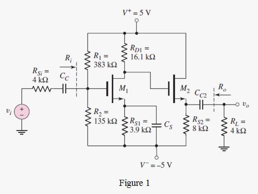
Consider the common source amplifier in cascade with a source follower circuit in Figure 1. Here, transistor M1 is operated in common-source configuration and M2 is operated in common-gate configuration.
The drain current and gate to source voltage of both the transistors are the same.
The drain current is given by,
The gate to source voltage is given by,
Considering the transistor M1 , the gate voltage for the transistor M1 is,
Substituting the resistance values from the circuit and the bias voltage, the gate voltage is obtained as,
Now, the source voltage is ,
Substituting the resistance value,
Thus, gate source voltage in terms of first transistor is ,
Substituting the expression for gate source voltage in (1), the drain current for transistor M1 in quiescent condition is,
On rearranging the above equation, the final quadratic equation is obtained as
Since the transistor is in saturation, the lower value among the two is considered. Hence, the drain current for the first transistor is,
Now, the drain to source voltage for the transistor M1 can be expressed as,
Substituting the values of parameters,
Considering the transistor M2, the gate voltage is same as the drain voltage of transistor M1, given by
The source voltage is given by,
The gate source voltage is therefore,
The drain current for transistor M2 is given by,
Solving the above expression, the final quadratic equation is obtained as,
Thus, the equation is given by,
Since the transistor is in saturation, the lower value among the two is considered. Hence, the drain current for the second transistor is,
Now, the drain to source voltage for the transistor M2 at Q-point can be expressed as,
Substituting the values of parameters,
(b)
The voltage gain of an NMOS cascade circuit with given transistor parameters.
Answer to Problem 4.12TYU
The voltage gain is given by
Explanation of Solution
Given Information:
:An NMOS cascade device with transistor parameters
Calculation:
Consider the common source amplifier in cascade with a source follower circuit in Figure 1. Here, transistor M1 is operated in common-source configuration and M2 is operated in common-gate configuration.
The voltage gain of the circuit is expressed as,
Here,
Now, the transconductance of the amplifier is given by,
Considering quiescent value of drain current,
Similarly, the transconductance of the second transistor is,
Substituting the transconductance values and the resistor values, the voltage gain is given by,
(c)
The output resistance of an NMOS cascade circuit with given transistor parameters.
Answer to Problem 4.12TYU
The output resistance is given by
Explanation of Solution
Given Information:
An NMOS cascade device with transistor parameters
Calculation:
The output resistance of the circuit is that of the output resistance of the emitter follower circuit which is low. It can be deduced from the small signal equivalent circuit shown below.
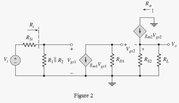
As it appears in the circuit, the output resistance of the circuit excluding the load resistance is obtained by considering the Kirchoff’s current law at the output node x which is,
This implies, the output resistance is given by,
Substituting the resistance and transconductance value,
Want to see more full solutions like this?
Chapter 4 Solutions
Microelectronics: Circuit Analysis and Design


- 18arrow_forward15arrow_forwardGiven the following, assume 0.7 V votlage drop across LEDs when they are positively biased.(a) When VB=0V, which LED is on?(b) When VB=5V, which LED is on?(c) If you want to limit the current through the LEDs to 10mA for both cases of 3(a) and 3 (b), find out the resistor values of RG and RR.arrow_forward
- Given the following, the intial condtion of output Q is high (H). (a) When /ALM is pushed on, creating a short to ground, what are the inputvoltages of S and R, and the output voltage Q?(b) After (a) happens, /ALM is released. What is the output voltage Q?(c) After (a) and (b) happen, /RESET is pushed on, creating a short to ground,what are the input voltages of S and R, and the output voltage Q?(d) After (a), (b) and (c) happen, /RESET is released. What is the output voltageQ?arrow_forwardHelp on this question about mass-spring system below?arrow_forwardAlso need help on this other mass-spring system belowarrow_forward
 Introductory Circuit Analysis (13th Edition)Electrical EngineeringISBN:9780133923605Author:Robert L. BoylestadPublisher:PEARSON
 Delmar's Standard Textbook Of ElectricityElectrical EngineeringISBN:9781337900348Author:Stephen L. HermanPublisher:Cengage Learning
 Programmable Logic ControllersElectrical EngineeringISBN:9780073373843Author:Frank D. PetruzellaPublisher:McGraw-Hill Education
 Fundamentals of Electric CircuitsElectrical EngineeringISBN:9780078028229Author:Charles K Alexander, Matthew SadikuPublisher:McGraw-Hill Education
 Electric Circuits. (11th Edition)Electrical EngineeringISBN:9780134746968Author:James W. Nilsson, Susan RiedelPublisher:PEARSON
 Engineering ElectromagneticsElectrical EngineeringISBN:9780078028151Author:Hayt, William H. (william Hart), Jr, BUCK, John A.Publisher:Mcgraw-hill Education,