Concept explainers
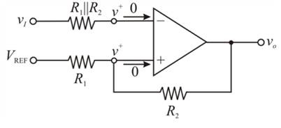
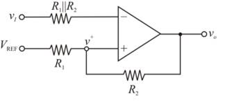
Consider the Schmitt trigger in Figure 15.30(a). (a) Derive the expressionfor the switching point and crossover voltages as given in Equations (15.76)and (15.77). (b) Let
(a)
To derive: the expression for the switching point and crossover voltages
Answer to Problem 15.49P
The switching voltage
The upper crossover voltage of Schmitt trigger is
The lower crossover voltage of Schmitt trigger is
Explanation of Solution
Given:
Consider the Schmitt trigger as shown below.

Calculation:
In an ideal op-amp, the inverting and non-inverting terminal currents are zero. And the inverting and non-inverting node voltages are equal. Given circuit can be represented as

Applying Kirchhoff’s current law at inverting node:
Applying Kirchhoff’s current law at non-inverting node:
Assuming
Therefore, the switching voltage
When
The upper crossover voltage off Schmitt trigger is
Therefore, the upper crossover voltage of Schmitt trigger is
When
The lower cross over voltage of Schmitt trigger is
Therefore, the lower crossover voltage of Schmitt trigger is
Conclusion:
The switching voltage
The upper crossover voltage of Schmitt trigger is
The lower crossover voltage of Schmitt trigger is
(b)
The values of
Answer to Problem 15.49P
The resistor values are
The reference voltage is
Explanation of Solution
Given:
The crossover voltages are
The minimum resistance is to be

Calculation:
Let
The minimum resistance is to be
The crossover voltages are
Substitute
Substitute
Substitute
Choose
Therefore, the resistor values are
Substitute
Substitute
Conclusion:
Therefore, the resistor values are
(c)
To find: the currents in the resistors when
Answer to Problem 15.49P
When
When
Explanation of Solution
Given:
Consider the Schmitt trigger as shown below.

Calculation:
The current in the resistor is given by
( i ) When
The current in the resistor is
Therefore, the current is
( ii ) When
The current in the resistor is
Therefore, the current is
Conclusion:
Therefore,
When
When
Want to see more full solutions like this?
Chapter 15 Solutions
Microelectronics: Circuit Analysis and Design
- 4) Find the valve of current if using nodal analys.3. (write and then solve the set of equations toget current Ex from your voltage variables.) M 3 ча + GA हुप 8Aarrow_forward2) Write but do not solve the set of Nodal equations for this circuit. 35 34 M x www 2 3A ↑ -+ 1v {7 ww 6 Bixarrow_forward3) Write: but do not solve the set of Nodal equations. for this circuit. m 4 13 35 23 ZA 5 M 8V (±) 6arrow_forward
- Feedback and open-loop gains. کا ✓ = B= S R1 ww C1 C2 R2 ww derive the oscillation frequency,arrow_forward1) Write but do not solve the set of Nodal equations for this circuit. 12 m 8 4A √3 ww www 6 ±7V 5 हुप Дам V 1 3 mmm 2Aarrow_forwardUse Gauss elimination method to find I₁, I2 and I, for the circuit shown below, if 60 12 Ω 80 13 4Ω 32V 16 Ωarrow_forward
- solve in detailarrow_forwardProblem 5 Plot the impulse response of the system shown below. Hint: This is done graphically with 4 convolutions. x[n] D y[n]< D D D D D D D D D D Darrow_forwardProblem 3 Assume that a[n] and y[n] satisfy the relation y[n] = −x[n−2]+h[n−2] * x[n+1] h[n] -3-2-10123 n where h[n] is shown in the figure. Can we equivalently write that y[n] = g[n] * x[n] for some sequence g[n] ? If so, plot g[n]. If not, explain why.arrow_forward
 Introductory Circuit Analysis (13th Edition)Electrical EngineeringISBN:9780133923605Author:Robert L. BoylestadPublisher:PEARSON
 Delmar's Standard Textbook Of ElectricityElectrical EngineeringISBN:9781337900348Author:Stephen L. HermanPublisher:Cengage Learning
 Programmable Logic ControllersElectrical EngineeringISBN:9780073373843Author:Frank D. PetruzellaPublisher:McGraw-Hill Education
 Fundamentals of Electric CircuitsElectrical EngineeringISBN:9780078028229Author:Charles K Alexander, Matthew SadikuPublisher:McGraw-Hill Education
 Electric Circuits. (11th Edition)Electrical EngineeringISBN:9780134746968Author:James W. Nilsson, Susan RiedelPublisher:PEARSON
 Engineering ElectromagneticsElectrical EngineeringISBN:9780078028151Author:Hayt, William H. (william Hart), Jr, BUCK, John A.Publisher:Mcgraw-hill Education,


