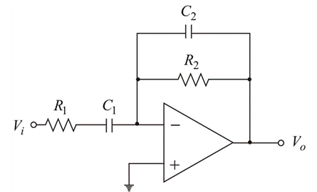
(a)
To derive: the expression for the voltage transfer function
(a)
Explanation of Solution
Given:

Calculation:
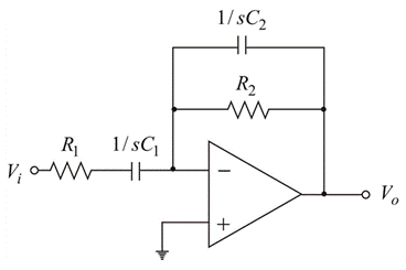
Redraw the given circuit in s -domain as

From the circuit,
Now the transfer function is
Hence
Thus, the required voltage transfer function is
Conclusion:
Thus, the required voltage transfer function is
(b)
To find: The value of
(b)
Answer to Problem 15.18P
The required values are
Explanation of Solution
Given:
Magnitude of the mid band gain is 50
Cut-off frequency
Cut-off frequency

Calculation:
Consider
The magnitude of the voltage transfer function is given by
Given
To determine the cut-off frequency
For
For
Let us consider
The equation (1) becomes,
From equation (2),
Substituting equation (5) in equation (4),
Substitute the values of
Hence the roots are obtained as
Since
Now, substitute the value of
Hence, by substituting the values
Further simplify as
Given
Therefore, the required resistor value is
Now
Therefore, the required capacitor
Conclusion:
Therefore, the required values are
Want to see more full solutions like this?
Chapter 15 Solutions
Microelectronics: Circuit Analysis and Design
- 2.80+4'selevision stations are to be transmited deough a single fiber optic cable using uncompressed PCM and TDM. Each station comprises one 22 kHz audio channel samplod at (1+0.24) times the Nyquist rate and encoded at a bit dop of 12 bSa, plan one 2.0 MHz video channel sampled at the mininum rite The video signal must be transmitted with an accuracy of better than (20 3) Find De (minimum) bit depth of the video signal. b) Find the bit rate associated with a single television station, including both audio and video e) Find the minimus bandwidth (the total multiplexed PCM signal.arrow_forward5. Consider a Shor who (4) Skh the impulse repom of the Chor for -5%, a-2+5. Omie weer de Sher is drain canal and explain sty odical, chronic sale of a hat will result in a coal for, and expls why itarrow_forwardFind the inverse Z-transform of X(z) using partial fraction method X(z) = z²+Z Z2-3Z+2 for i) ROC 12 iii) ROC |z| <1arrow_forward
- .The previous solution does not explain the steps Consider the signal: f(t) = 글씨를 1 0, otherwise Use the Fourier transform formula to find F(w).arrow_forward3. Find the transfer function and show all steps.arrow_forward8. Determine the center frequency and Bandwidth of the following bandpass filter, show all steps.arrow_forward
- 5. Find the Transfer Function of the following circuit. Prove that it’s a low pass filter, show all steps.arrow_forward2. Find the transfer function, show all steps.arrow_forwardI have this fsk function code: function [x]=fsk_encode(b,s,f0,f1,N,Fs,K) % b= bit sequence vector % s(1)= output level for 0 % s(2)= output level for 1 % N= length of bit sequence % Fs= Sampling frequency y=zeros(1,N*K); %Setup output vector %for each bit calculatee the rando samples for n=1:N for k=1:K t = (k - 1) / Fs; if(b(n)==0) y((n-1)*K+k)=cos(2*pi*f0*t); % pulse=0 else y((n-1)*K+k)=cos(2*pi*f1*t); % pulse=1 end end x=y; %set output end And this is another code that calls the function in order to get the power density spectrum: clc;clear; % EE 382 Communication Systems- Lab 8 % Plots the power spectrum of the ASK modulation % First specify some parameters N=256; % number of bits per realization M=100; % number of realizations in the ensemble T=0.001; % bit duration in seconds delf =2e+3; fc=10e+3; f0=fc-delf; f1=fc+delf; Fs=8*f1; % sampling frequency (this is needed to calibrate the frequency axis) K=(T/(1/Fs)); % Define arrays for bit sequences and sampled waveforms…arrow_forward
 Introductory Circuit Analysis (13th Edition)Electrical EngineeringISBN:9780133923605Author:Robert L. BoylestadPublisher:PEARSON
 Delmar's Standard Textbook Of ElectricityElectrical EngineeringISBN:9781337900348Author:Stephen L. HermanPublisher:Cengage Learning
 Programmable Logic ControllersElectrical EngineeringISBN:9780073373843Author:Frank D. PetruzellaPublisher:McGraw-Hill Education
 Fundamentals of Electric CircuitsElectrical EngineeringISBN:9780078028229Author:Charles K Alexander, Matthew SadikuPublisher:McGraw-Hill Education
 Electric Circuits. (11th Edition)Electrical EngineeringISBN:9780134746968Author:James W. Nilsson, Susan RiedelPublisher:PEARSON
 Engineering ElectromagneticsElectrical EngineeringISBN:9780078028151Author:Hayt, William H. (william Hart), Jr, BUCK, John A.Publisher:Mcgraw-hill Education,


