
MICROELECT. CIRCUIT ANALYSIS&DESIGN (LL)
4th Edition
ISBN: 9781266368622
Author: NEAMEN
Publisher: MCG
expand_more
expand_more
format_list_bulleted
Concept explainers
Videos
Textbook Question
Chapter 1, Problem 1.39P
Consider the diode circuit shown in Figure P1.39. The diode reverse−saturation current is
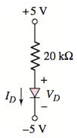
Figure P1.39
Expert Solution & Answer
Want to see the full answer?
Check out a sample textbook solution
Students have asked these similar questions
use this code on the bottom to answer the question in the photo
clc; clearvars;
% Read the file [y, Fs] = audioread('106miles.wav'); N = length(y); Nfft = 2^nextpow2(N); dt = 1/Fs; t = (0:dt:(N-1)*dt)'; % Ensure t is a column vector y = y - mean(y); % Remove DC component (if not already zero-mean)
% Carrier signal (25 kHz) fc = 25000; % Carrier frequency in Hz carrier = cos(2 * pi * fc * t);
% DSB-SC Modulation modulated_signal = y .* carrier;
% Plot Time Domain Signal figure; subplot(2,1,1); plot(t, y); title('Original Signal (Time Domain)'); xlabel('Time (s)'); ylabel('Amplitude');
subplot(2,1,2); plot(t, modulated_signal); title('DSB-SC Modulated Signal (Time Domain)'); xlabel('Time (s)'); ylabel('Amplitude');
% Frequency Domain (FFT) Y = fft(y, Nfft) / Nfft; Modulated_Y = fft(modulated_signal, Nfft) / Nfft; f = Fs * (0:(Nfft/2)) / Nfft; % Frequency vector
% Plot Frequency Domain Signal figure; subplot(2,1,1); plot(f, abs(Y(1:Nfft/2+1))); title('Original Signal…
5-9 A 230 V shunt motor has a nominal arma-
ture current of 60 A. If the armature resist-
ance is 0.152, calculate the following:
a. The counter-emf [V]
b. The power supplied to the armature [W]
c. The mechanical power developed by the
motor, [kW] and [hp]
5-10 a. In Problem 5-9 calculate the initial start-
ing current if the motor is directly con-
nected across the 230 V line.
b. Calculate the value of the starting resistor
needed to limit the initial current to 115 A.
how to solve this?
Chapter 1 Solutions
MICROELECT. CIRCUIT ANALYSIS&DESIGN (LL)
Ch. 1 - Calculate the intrinsic carrier concentration in...Ch. 1 - (a) Calculate the majority and minority carrier...Ch. 1 - Consider ntype GaAs at T=300K doped to a...Ch. 1 - Consider silicon at T=300K . Assume the hole...Ch. 1 - Determine the intrinsic carrier concentration in...Ch. 1 - (a) Consider silicon at T=300K . Assume that...Ch. 1 - Using the results of TYU1.2, determine the drift...Ch. 1 - The electron and hole diffusion coefficients in...Ch. 1 - A sample of silicon at T=300K is doped to...Ch. 1 - (a) Calculate Vbi for a GaAs pn junction at T=300K...
Ch. 1 - A silicon pn junction at T=300K is doped at...Ch. 1 - (a) A silicon pn junction at T=300K has a...Ch. 1 - (a) Determine Vbi for a silicon pn junction at...Ch. 1 - A silicon pn junction diode at T=300K has a...Ch. 1 - Recall that the forwardbias diode voltage...Ch. 1 - Consider the circuit in Figure 1.28. Let VPS=4V ,...Ch. 1 - (a) Consider the circuit shown in Figure 1.28. Let...Ch. 1 - The resistor parameter in the circuit shown in...Ch. 1 - Consider the diode and circuit in Exercise EX 1.8....Ch. 1 - Consider the circuit in Figure 1.28. Let R=4k and...Ch. 1 - The power supply (input) voltage in the circuit of...Ch. 1 - (a) The circuit and diode parameters for the...Ch. 1 - Determine the diffusion conductance of a pn...Ch. 1 - Determine the smallsignal diffusion resistance of...Ch. 1 - The diffusion resistance of a pn junction diode at...Ch. 1 - A pn junction diode and a Schottky diode both have...Ch. 1 - Consider the circuit shown in Figure 1.45....Ch. 1 - Consider the circuit shown in Figure 1.46. The...Ch. 1 - A Zener diode has an equivalent series resistance...Ch. 1 - The resistor in the circuit shown in Figure 1.45...Ch. 1 - Describe an intrinsic semiconductor material. What...Ch. 1 - Describe the concept of an electron and a hole as...Ch. 1 - Describe an extrinsic semiconductor material. What...Ch. 1 - Describe the concepts of drift current and...Ch. 1 - How is a pn junction formed? What is meant by a...Ch. 1 - How is a junction capacitance created in a...Ch. 1 - Write the ideal diode currentvoltage relationship....Ch. 1 - Describe the iteration method of analysis and when...Ch. 1 - Describe the piecewise linear model of a diode and...Ch. 1 - Define a load line in a simple diode circuit.Ch. 1 - Under what conditions is the smallsignal model of...Ch. 1 - Describe the operation of a simple solar cell...Ch. 1 - How do the i characteristics of a Schottky barrier...Ch. 1 - What characteristic of a Zener diode is used in...Ch. 1 - Describe the characteristics of a photodiode and a...Ch. 1 - (a) Calculate the intrinsic carrier concentration...Ch. 1 - (a) The intrinsic carrier concentration in silicon...Ch. 1 - Calculate the intrinsic carrier concentration in...Ch. 1 - (a) Find the concentration of electrons and holes...Ch. 1 - Gallium arsenide is doped with acceptor impurity...Ch. 1 - Silicon is doped with 51016 arsenic atoms/cm3 ....Ch. 1 - (a) Calculate the concentration of electrons and...Ch. 1 - A silicon sample is fabricated such that the hole...Ch. 1 - The electron concentration in silicon at T=300K is...Ch. 1 - (a) A silicon semiconductor material is to be...Ch. 1 - (a) The applied electric field in ptype silicon is...Ch. 1 - A drift current density of 120A/cm2 is established...Ch. 1 - An ntype silicon material has a resistivity of...Ch. 1 - (a) The applied conductivity of a silicon material...Ch. 1 - In GaAs, the mobilities are n=8500cm2/Vs and...Ch. 1 - The electron and hole concentrations in a sample...Ch. 1 - The hole concentration in silicon is given by...Ch. 1 - GaAs is doped to Na=1017cm3 . (a) Calculate no and...Ch. 1 - (a) Determine the builtin potential barrier Vbi in...Ch. 1 - Consider a silicon pn junction. The nregion is...Ch. 1 - The donor concentration in the nregion of a...Ch. 1 - Consider a uniformly doped GaAs pn junction with...Ch. 1 - The zerobiased junction capacitance of a silicon...Ch. 1 - The zerobias capacitance of a silicon pn junction...Ch. 1 - The doping concentrations in a silicon pn junction...Ch. 1 - (a) At what reversebias voltage does the...Ch. 1 - (a) The reversesaturation current of a pn junction...Ch. 1 - (a) The reversesaturation current of a pn junction...Ch. 1 - A silicon pn junction diode has an emission...Ch. 1 - Plot log10ID versus VD over the range 0.1VD0.7V...Ch. 1 - (a) Consider a silicon pn junction diode operating...Ch. 1 - A pn junction diode has IS=2nA . (a) Determine the...Ch. 1 - The reversebias saturation current for a set of...Ch. 1 - A germanium pn junction has a diode current of...Ch. 1 - (a)The reversesaturation current of a gallium...Ch. 1 - The reversesaturation current of a silicon pn...Ch. 1 - A silicon pn junction diode has an applied...Ch. 1 - A pn junction diode is in series with a 1M...Ch. 1 - Consider the diode circuit shown in Figure P1.39....Ch. 1 - The diode in the circuit shown in Figure P1.40 has...Ch. 1 - Prob. 1.41PCh. 1 - (a) The reversesaturation current of each diode in...Ch. 1 - (a) Consider the circuit shown in Figure P1.40....Ch. 1 - Consider the circuit shown in Figure P1.44....Ch. 1 - The cutin voltage of the diode shown in the...Ch. 1 - Find I and VO in each circuit shown in Figure...Ch. 1 - Repeat Problem 1.47 if the reversesaturation...Ch. 1 - (a) In the circuit Shown in Figure P1.49, find the...Ch. 1 - Assume each diode in the circuit shown in Figure...Ch. 1 - (a) Consider a pn junction diode biased at IDQ=1mA...Ch. 1 - Determine the smallsignal diffusion resistancefor...Ch. 1 - The diode in the circuit shown in Figure P1.53 is...Ch. 1 - The forwardbias currents in a pn junction diode...Ch. 1 - A pn junction diode and a Schottky diode have...Ch. 1 - The reversesaturation currents of a Schottky diode...Ch. 1 - Consider the Zener diode circuit shown in Figure...Ch. 1 - (a) The Zener diode in Figure P1.57 is ideal with...Ch. 1 - Consider the Zener diode circuit shown in Figure...Ch. 1 - The Output current of a pn junction diode used as...Ch. 1 - Using the currentvoltage characteristics of the...Ch. 1 - (a) Using the currentvoltage characteristics of...Ch. 1 - Use a computer simulation to generate the ideal...Ch. 1 - Use a computer simulation to find the diode...Ch. 1 - Design a diode circuit to produce the load line...Ch. 1 - Design a circuit to produce the characteristics...Ch. 1 - Design a circuit to produce the characteristics...Ch. 1 - Design a circuit to produce the characteristics...
Knowledge Booster


Learn more about
Need a deep-dive on the concept behind this application? Look no further. Learn more about this topic, electrical-engineering and related others by exploring similar questions and additional content below.Similar questions
- For the circuit in Fig. P8.52, choose the load impedance ZLso that the power dissipated in it is a maximum. How much powerwill that be?arrow_forwardhow to solve the attached question? please explain or give reference where required in the solution.arrow_forwardHANDWRITTEN SOLUTION REQUIRED NOT USING CHATGPTarrow_forward
- Please only do part E and F. Please show your work and be as detailed as possible. Please explain the relationship between K the gain and stability of the system. Also, show how to plot the poles and why they are on either the real or imaginary axis. What is it about the example that indicated that? thank youarrow_forwardPlease draw the block diagram for this problem and explain how. thank youarrow_forwardPlease show your work and be as detailed as possible. I would like to really understand the connection between the type of loop, the dampness, and the gain, K. Thank youarrow_forward
- In the zone refining of silicon, an RF-heater is used to remove trace amounts of impuritiesfrom the silicon. If the silicon has the impurity of 10^14 Co (k = 8*10^-6) what is the purityof the crystal after one pass of the zone refiner? After two passes? Plot concentration as afunction of crystal length from 0 to 8ft (total length of the crystal). The width of the moltenzone is 5”.arrow_forwardNot use ai pleasearrow_forwardSolve on paper not using AI or chatgptarrow_forward
- Can you solve for V1 and V2arrow_forwardyou dont need to solve the question i just wanna know the steps and how to find the angle between the voltage difference and the current . thanks so mucharrow_forwardistics of diodes, bipolar junction transistors, and plain the structure, operation, 1. The purpose of doping in semiconductor diodes is: a) To control their electrical properties b) To increase their physical size c) To enhance their mechanical strength d) To improve their thermal stability 2. In electronics production, your team wants to manufacture a very cheap diode rectifier. Which of the following rectifier configurations would you select? a) Half-wave rectifier c) Full-wave rectifier b) Bridge rectifier d) Controlled rectifier 3. The region that a Zener diode operates to provide voltage regulation is: a) Saturation c) Reverse bias b) Breakdown d) Forward bias 4. In NMOS transistors, the depth of the channel is primarily changed by: a) VDS b) lp c) VGS d) None of these 5. NMOS transistors have than PMOS, resulting in better current conduction: b) Long channel a) High mobility c) Low mobility d) Short channel 6. You are working in electronic production, and your team is asked to…arrow_forward
arrow_back_ios
SEE MORE QUESTIONS
arrow_forward_ios
Recommended textbooks for you

Diodes Explained - The basics how diodes work working principle pn junction; Author: The Engineering Mindset;https://www.youtube.com/watch?v=Fwj_d3uO5g8;License: Standard Youtube License