
MICROELECT. CIRCUIT ANALYSIS&DESIGN (LL)
4th Edition
ISBN: 9781266368622
Author: NEAMEN
Publisher: MCG
expand_more
expand_more
format_list_bulleted
Concept explainers
Textbook Question
Chapter 1, Problem D1.69DP
Design a circuit to produce the characteristics shown in Figure P1.69, where
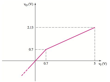
Figure P1.69
Expert Solution & Answer
Want to see the full answer?
Check out a sample textbook solution
Students have asked these similar questions
Q2. For the transformer shown in Fig. 1.
A. Plot the winding connection for the transformer and justify your answer.
(4M)
B. If the transformer is adopted in 12 pulse diode rectifier, where two-series connected
bridge rectifiers are used to supply a highly inductive load with 100 A. (i) Select a
suitable turns ratio for the transformer (ii) Plot the line current of each winding (
secondary + primary) showing the current magnitude at each interval (iii) Use Fourier
Page 1 of 3
analysis to obtain the Fourier series of all line currents then calculate the THD of the
input current.
(8=0°
(16M)
(Y) = 30°
Fig. 1
P. I v
I
Q2. For the transformer shown in Fig.1,
A. Find the phase shift between the primary and star-connected secondary.
B. If the transformer is adopted in a 12-pulse diode rectifier, where a two-series
connected bridge rectifier is connected in series and supplies a highly inductive load
(i) Select a suitable turns ratio for the transformer
(ii) Plot the line current of each winding (secondary + primary).
(iii)Using Fourier analysis to obtain the Fourier series of all line currents, then calculate
the THD of the input current.
(iv) Draw the output voltage of the first and second rectifiers and give the relation of
the total output voltage.
N2
B
C
Fig. 1
N3
a
Q2.A. It is planned to use the transformer shown in Fig. 1, a 12-pulse rectifier. Each
secondary is connected to three phase controlled bridge rectifier. The two rectifiers
are connected in series to supply a highly inductive load.
1. Based on the phasor relationship between different windings. If suitable turns
ratio is selected, is it possible to use this transformer to produce 12 pulse
output voltage? Show the reason behind your answer.
2. Assuming this arrangement is possible to be used in 12-pulse rectifier, draw
the output voltage of the 1st and 2nd rectifier and give the relation of the total
output voltage.
3. Use the Fourier analysis to show the harmonics in all line currents of the
transformer.
A
B
in
C
Fig. 1
b
la
a
2
b.
Chapter 1 Solutions
MICROELECT. CIRCUIT ANALYSIS&DESIGN (LL)
Ch. 1 - Calculate the intrinsic carrier concentration in...Ch. 1 - (a) Calculate the majority and minority carrier...Ch. 1 - Consider ntype GaAs at T=300K doped to a...Ch. 1 - Consider silicon at T=300K . Assume the hole...Ch. 1 - Determine the intrinsic carrier concentration in...Ch. 1 - (a) Consider silicon at T=300K . Assume that...Ch. 1 - Using the results of TYU1.2, determine the drift...Ch. 1 - The electron and hole diffusion coefficients in...Ch. 1 - A sample of silicon at T=300K is doped to...Ch. 1 - (a) Calculate Vbi for a GaAs pn junction at T=300K...
Ch. 1 - A silicon pn junction at T=300K is doped at...Ch. 1 - (a) A silicon pn junction at T=300K has a...Ch. 1 - (a) Determine Vbi for a silicon pn junction at...Ch. 1 - A silicon pn junction diode at T=300K has a...Ch. 1 - Recall that the forwardbias diode voltage...Ch. 1 - Consider the circuit in Figure 1.28. Let VPS=4V ,...Ch. 1 - (a) Consider the circuit shown in Figure 1.28. Let...Ch. 1 - The resistor parameter in the circuit shown in...Ch. 1 - Consider the diode and circuit in Exercise EX 1.8....Ch. 1 - Consider the circuit in Figure 1.28. Let R=4k and...Ch. 1 - The power supply (input) voltage in the circuit of...Ch. 1 - (a) The circuit and diode parameters for the...Ch. 1 - Determine the diffusion conductance of a pn...Ch. 1 - Determine the smallsignal diffusion resistance of...Ch. 1 - The diffusion resistance of a pn junction diode at...Ch. 1 - A pn junction diode and a Schottky diode both have...Ch. 1 - Consider the circuit shown in Figure 1.45....Ch. 1 - Consider the circuit shown in Figure 1.46. The...Ch. 1 - A Zener diode has an equivalent series resistance...Ch. 1 - The resistor in the circuit shown in Figure 1.45...Ch. 1 - Describe an intrinsic semiconductor material. What...Ch. 1 - Describe the concept of an electron and a hole as...Ch. 1 - Describe an extrinsic semiconductor material. What...Ch. 1 - Describe the concepts of drift current and...Ch. 1 - How is a pn junction formed? What is meant by a...Ch. 1 - How is a junction capacitance created in a...Ch. 1 - Write the ideal diode currentvoltage relationship....Ch. 1 - Describe the iteration method of analysis and when...Ch. 1 - Describe the piecewise linear model of a diode and...Ch. 1 - Define a load line in a simple diode circuit.Ch. 1 - Under what conditions is the smallsignal model of...Ch. 1 - Describe the operation of a simple solar cell...Ch. 1 - How do the i characteristics of a Schottky barrier...Ch. 1 - What characteristic of a Zener diode is used in...Ch. 1 - Describe the characteristics of a photodiode and a...Ch. 1 - (a) Calculate the intrinsic carrier concentration...Ch. 1 - (a) The intrinsic carrier concentration in silicon...Ch. 1 - Calculate the intrinsic carrier concentration in...Ch. 1 - (a) Find the concentration of electrons and holes...Ch. 1 - Gallium arsenide is doped with acceptor impurity...Ch. 1 - Silicon is doped with 51016 arsenic atoms/cm3 ....Ch. 1 - (a) Calculate the concentration of electrons and...Ch. 1 - A silicon sample is fabricated such that the hole...Ch. 1 - The electron concentration in silicon at T=300K is...Ch. 1 - (a) A silicon semiconductor material is to be...Ch. 1 - (a) The applied electric field in ptype silicon is...Ch. 1 - A drift current density of 120A/cm2 is established...Ch. 1 - An ntype silicon material has a resistivity of...Ch. 1 - (a) The applied conductivity of a silicon material...Ch. 1 - In GaAs, the mobilities are n=8500cm2/Vs and...Ch. 1 - The electron and hole concentrations in a sample...Ch. 1 - The hole concentration in silicon is given by...Ch. 1 - GaAs is doped to Na=1017cm3 . (a) Calculate no and...Ch. 1 - (a) Determine the builtin potential barrier Vbi in...Ch. 1 - Consider a silicon pn junction. The nregion is...Ch. 1 - The donor concentration in the nregion of a...Ch. 1 - Consider a uniformly doped GaAs pn junction with...Ch. 1 - The zerobiased junction capacitance of a silicon...Ch. 1 - The zerobias capacitance of a silicon pn junction...Ch. 1 - The doping concentrations in a silicon pn junction...Ch. 1 - (a) At what reversebias voltage does the...Ch. 1 - (a) The reversesaturation current of a pn junction...Ch. 1 - (a) The reversesaturation current of a pn junction...Ch. 1 - A silicon pn junction diode has an emission...Ch. 1 - Plot log10ID versus VD over the range 0.1VD0.7V...Ch. 1 - (a) Consider a silicon pn junction diode operating...Ch. 1 - A pn junction diode has IS=2nA . (a) Determine the...Ch. 1 - The reversebias saturation current for a set of...Ch. 1 - A germanium pn junction has a diode current of...Ch. 1 - (a)The reversesaturation current of a gallium...Ch. 1 - The reversesaturation current of a silicon pn...Ch. 1 - A silicon pn junction diode has an applied...Ch. 1 - A pn junction diode is in series with a 1M...Ch. 1 - Consider the diode circuit shown in Figure P1.39....Ch. 1 - The diode in the circuit shown in Figure P1.40 has...Ch. 1 - Prob. 1.41PCh. 1 - (a) The reversesaturation current of each diode in...Ch. 1 - (a) Consider the circuit shown in Figure P1.40....Ch. 1 - Consider the circuit shown in Figure P1.44....Ch. 1 - The cutin voltage of the diode shown in the...Ch. 1 - Find I and VO in each circuit shown in Figure...Ch. 1 - Repeat Problem 1.47 if the reversesaturation...Ch. 1 - (a) In the circuit Shown in Figure P1.49, find the...Ch. 1 - Assume each diode in the circuit shown in Figure...Ch. 1 - (a) Consider a pn junction diode biased at IDQ=1mA...Ch. 1 - Determine the smallsignal diffusion resistancefor...Ch. 1 - The diode in the circuit shown in Figure P1.53 is...Ch. 1 - The forwardbias currents in a pn junction diode...Ch. 1 - A pn junction diode and a Schottky diode have...Ch. 1 - The reversesaturation currents of a Schottky diode...Ch. 1 - Consider the Zener diode circuit shown in Figure...Ch. 1 - (a) The Zener diode in Figure P1.57 is ideal with...Ch. 1 - Consider the Zener diode circuit shown in Figure...Ch. 1 - The Output current of a pn junction diode used as...Ch. 1 - Using the currentvoltage characteristics of the...Ch. 1 - (a) Using the currentvoltage characteristics of...Ch. 1 - Use a computer simulation to generate the ideal...Ch. 1 - Use a computer simulation to find the diode...Ch. 1 - Design a diode circuit to produce the load line...Ch. 1 - Design a circuit to produce the characteristics...Ch. 1 - Design a circuit to produce the characteristics...Ch. 1 - Design a circuit to produce the characteristics...
Knowledge Booster
Learn more about
Need a deep-dive on the concept behind this application? Look no further. Learn more about this topic, electrical-engineering and related others by exploring similar questions and additional content below.Similar questions
- Q4. Give the reasons for the following 1. In AC machines drives, the frequency modulation index should be integer regardless the value of switching frequency. 2. Variable de link voltage is adopted in inverter operating in square wave operation mode 3. Practical values of switch utilization factor is different from theoretical values 4. In three-phase inverter with my is odd and multiple of 3, the even and tripplen harmonics are zero. 5. The PSC-PWM is attractive for the modular multilevel converterarrow_forwardQ6.B. Answer the following questions 1. Does the steady state load current in a half bridge inverter has an average value and what is the adverse effect of the average current component? 2. Can the LPF of single phase bridge inverter based on bipolar PWM be used with single phase bridge inverter based on unipolar PWM? Explainarrow_forwardQ3. Answer the following questions T 1. Compared to the bipolar voltage-switching scheme, the unipolar scheme is "effectively" doubling the switching frequency. Explain the statement's meaning and how this effect can be generated. 2. What are the properties of a good power switch, and what are its basic ratings? 3. What are the objectives of any PWM strategy for three-phase inverters? 4. Why is the current control PWM rectifier in the dq rotating reference frame preferred over the abc reference frame? 5. Define the switch utilization factor. Show how this factor can be calculated for different single-phase inverters for square wave operation mode at the maximum rated output.arrow_forward
- Q1.B. Explain output control by voltage cancellation in a single-phase inverter. What are the advantages over square wave operation?arrow_forwardQ3.B. What is the problem of three-phase HW rectifier and how can be resolved?arrow_forwardQ3-consider the unity feedback system shown below: a.Evaluate general formula of ess? b.Calculate the steady state error of the closed loop system due to R(s) unit step input, D(s)=0]? c.Calculate the steady-state response when D(s) and ramp and R(s)=0?arrow_forward
- - = 400KHZ. Q1. In a Boost converter, L = 25 μH, Vin = 12 V, D = 0.4, P = 25 W, and fs (i) if the output load is changing. Calculate the critical value of the output load P,below which the converter will enter the discontinuous conduction mode of operation. Assume the total turn-on loss is equal to 2 W. (ii) Assuming the input voltage fluctuates from 10 V to 14 V and the output voltage is regulated to 20 V. Calculate the critical value of the inductance L below which this Boost converter will enter the discontinuous conduction mode of operation at P = 5 W. (iii) Draw the waveforms for inductor voltage, inductor current, and the capacitor current for this Boost converter at the output load that causes it to operate at the border of continuous and discontinuous modes. vd tow 77 N₂ AT 22 1-1arrow_forwardDon't use ai to answer I will report you answerarrow_forwardAnswer the following questions: 1- Write radiation resistance (R.) equation for infinitesimal dipole antenna. 2- Write the angle expression form of first null beam width (FNBW) for 2/2 dipole. 3- Define the Directivity of antenna. 4- Write radar cross section equation. 5- Write the input impedance (Z) expression of lossless transmission line.arrow_forward
arrow_back_ios
SEE MORE QUESTIONS
arrow_forward_ios
Recommended textbooks for you

 Delmar's Standard Textbook Of ElectricityElectrical EngineeringISBN:9781337900348Author:Stephen L. HermanPublisher:Cengage Learning
 Electricity for Refrigeration, Heating, and Air C...Mechanical EngineeringISBN:9781337399128Author:Russell E. SmithPublisher:Cengage Learning


Delmar's Standard Textbook Of Electricity
Electrical Engineering
ISBN:9781337900348
Author:Stephen L. Herman
Publisher:Cengage Learning

Electricity for Refrigeration, Heating, and Air C...
Mechanical Engineering
ISBN:9781337399128
Author:Russell E. Smith
Publisher:Cengage Learning
Diodes Explained - The basics how diodes work working principle pn junction; Author: The Engineering Mindset;https://www.youtube.com/watch?v=Fwj_d3uO5g8;License: Standard Youtube License