MICROELECT. CIRCUIT ANALYSIS&DESIGN (LL)
4th Edition
ISBN: 9781266368622
Author: NEAMEN
Publisher: MCG
bartleby

Videos

Textbook Question
Book Icon
Chapter 1, Problem 1.47P

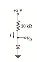
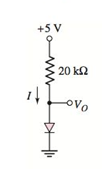
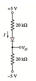
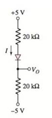
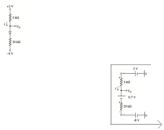
Find I and V O in each circuit shown in Figure P1.47 if (i) V γ = 0.7 V and (ii) V γ = 0.6 V .

  1. Chapter 1, Problem 1.47P, Find I and VO in each circuit shown in Figure P1.47 if (i) V=0.7V and (ii) V=0.6V . Figure P1.47 , example  1

  • Chapter 1, Problem 1.47P, Find I and VO in each circuit shown in Figure P1.47 if (i) V=0.7V and (ii) V=0.6V . Figure P1.47 , example  2
  • Chapter 1, Problem 1.47P, Find I and VO in each circuit shown in Figure P1.47 if (i) V=0.7V and (ii) V=0.6V . Figure P1.47 , example  3
  • Chapter 1, Problem 1.47P, Find I and VO in each circuit shown in Figure P1.47 if (i) V=0.7V and (ii) V=0.6V . Figure P1.47 , example  4
  • Figure P1.47

    (a).

    Expert Solution
    Check Mark
    To determine

    The values of I and Vo in the given circuit.

    Answer to Problem 1.47P

    For Vγ=0.7V , I=0.215mA,Vo=0.7V .

    For Vγ=0.6V , I=0.22mA,Vo=0.6V .

    Explanation of Solution

    Given Information:

    The given circuit is shown below.
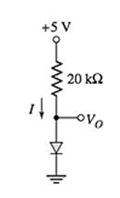
      MICROELECT. CIRCUIT ANALYSIS&DESIGN (LL), Chapter 1, Problem 1.47P , additional homework tip  1

    Two values of Vγ are

      Vγ=0.7VVγ=0.6V

    Calculation:

    For Vγ=0.7V ,

    The given circuit diagram is:

      MICROELECT. CIRCUIT ANALYSIS&DESIGN (LL), Chapter 1, Problem 1.47P , additional homework tip  2

    Assuming the diode is in ON state and the modified circuit is:
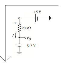
      MICROELECT. CIRCUIT ANALYSIS&DESIGN (LL), Chapter 1, Problem 1.47P , additional homework tip  3

    Applying Kirchhoff’s voltage law:

      5+I(20k)+0.7=0I=50.720kI=0.215mA

    The direction of current is from p-region to n-region of diode. Hence, the assumption is correct.

    Applying Kirchhoff’s voltage law:
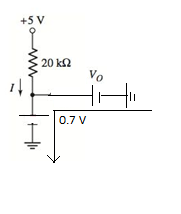
      MICROELECT. CIRCUIT ANALYSIS&DESIGN (LL), Chapter 1, Problem 1.47P , additional homework tip  4

      Vo+0.7V=0Vo=0.7V

    For Vγ=0.6V ,

    The given circuit diagram is:

      MICROELECT. CIRCUIT ANALYSIS&DESIGN (LL), Chapter 1, Problem 1.47P , additional homework tip  5

    Assuming the diode is in ON state and the modified circuit is:
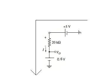
      MICROELECT. CIRCUIT ANALYSIS&DESIGN (LL), Chapter 1, Problem 1.47P , additional homework tip  6

    Applying Kirchhoff’s voltage law:

      5+I(20k)+0.6=0I=50.620kI=0.22mA

    The direction of current is from p-region to n-region of diode. Hence, the assumption is correct.

    Applying Kirchhoff’s voltage law:
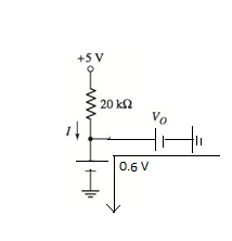
      MICROELECT. CIRCUIT ANALYSIS&DESIGN (LL), Chapter 1, Problem 1.47P , additional homework tip  7

      Vo+0.6V=0Vo=0.6V

    (b).

    Expert Solution
    Check Mark
    To determine

    The values of I and Vo in the given circuit.

    Answer to Problem 1.47P

    For Vγ=0.7V , I=0.2325mA,Vo=0.35V .

    For Vγ=0.6V , I=0.235mA,Vo=0.3V .

    Explanation of Solution

    Given Information:

    The given circuit is shown below.
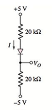
      MICROELECT. CIRCUIT ANALYSIS&DESIGN (LL), Chapter 1, Problem 1.47P , additional homework tip  8

    Two values of Vγ are

      Vγ=0.7VVγ=0.6V

    Calculation:

    For Vγ=0.7V ,

    The given circuit diagram is:

      MICROELECT. CIRCUIT ANALYSIS&DESIGN (LL), Chapter 1, Problem 1.47P , additional homework tip  9

    Assuming the diode is in ON state and the modified circuit is:
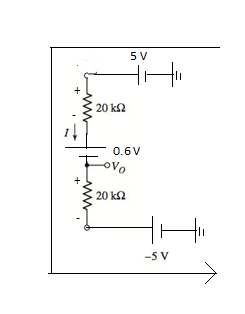
      MICROELECT. CIRCUIT ANALYSIS&DESIGN (LL), Chapter 1, Problem 1.47P , additional homework tip  10

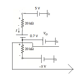
    Applying Kirchhoff’s voltage law:

      5+I(20k)+0.7+I(20k)+(5)=0(40k)I=100.7I=9.340kI=0.2325mA

    The direction of current is from p-region to n-region of diode. Hence, the assumption is correct.

    Applying Kirchhoff’s voltage law in the following circuit:
      MICROELECT. CIRCUIT ANALYSIS&DESIGN (LL), Chapter 1, Problem 1.47P , additional homework tip  11

      Vo+I(20k)+(5)=0Vo=(0.2325mA)(20k)5Vo=4.655Vo=0.35V

    For Vγ=0.6V ,

    The given circuit diagram is:

      MICROELECT. CIRCUIT ANALYSIS&DESIGN (LL), Chapter 1, Problem 1.47P , additional homework tip  12

    Assuming the diode is in ON state and the modified circuit is:

    Applying Kirchhoff’s voltage law:

      5+I(20k)+0.6+I(20k)+(5)=0(40k)I=100.6I=9.440kI=0.235mA

    The direction of current is from p-region to n-region of diode. Hence, the assumption is correct.

    Applying Kirchhoff’s voltage law in the following circuit:
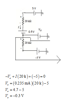
      MICROELECT. CIRCUIT ANALYSIS&DESIGN (LL), Chapter 1, Problem 1.47P , additional homework tip  13

    (c)

    Expert Solution
    Check Mark
    To determine

    The values of I and Vo in the given circuit.

    Answer to Problem 1.47P

    For Vγ=0.7V , I=0.372mA,Vo=0.14V

    For Vγ=0.6V , I=0.376mA,Vo=0.12V

    Explanation of Solution

    Given Information:

    The given circuit is shown below.

      MICROELECT. CIRCUIT ANALYSIS&DESIGN (LL), Chapter 1, Problem 1.47P , additional homework tip  14

    Two values of Vγ are

      Vγ=0.7VVγ=0.6V

    Calculation:

    For Vγ=0.7V ,

    The given circuit diagram is:

      MICROELECT. CIRCUIT ANALYSIS&DESIGN (LL), Chapter 1, Problem 1.47P , additional homework tip  15

    Assuming the diode is in ON state and the modified circuit is :

    Applying Kirchhoff’s voltage law:

      2+I(5k)+0.7+I(20k)+(8)=0(25k)I=100.7I=9.325kI=0.372mA

    The direction of current is from p-region to n-region of diode. Hence, the assumption is correct.

    Applying Kirchhoff’s voltage law in the following circuit:
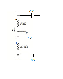
      MICROELECT. CIRCUIT ANALYSIS&DESIGN (LL), Chapter 1, Problem 1.47P , additional homework tip  16

      Vo+0.7+I(20k)+(8)=0Vo=0.7+(0.372mA)(20k)8Vo=7.3+7.44Vo=0.14V

    For Vγ=0.6V

    The given circuit diagram is:

      MICROELECT. CIRCUIT ANALYSIS&DESIGN (LL), Chapter 1, Problem 1.47P , additional homework tip  17

    Assuming the diode is in ON state and the modified circuit is:
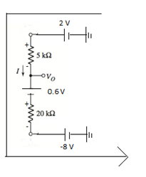
      MICROELECT. CIRCUIT ANALYSIS&DESIGN (LL), Chapter 1, Problem 1.47P , additional homework tip  18

    Applying Kirchhoff’s voltage law:

      2+I(5k)+0.6+I(20k)+(8)=0(25k)I=100.6I=9.425kI=0.376mA

    The direction of current is from p-region to n-region of diode. Hence, the assumption is correct.

    Applying Kirchhoff’s voltage law in the following circuit:
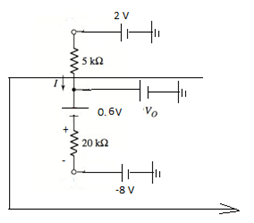
      MICROELECT. CIRCUIT ANALYSIS&DESIGN (LL), Chapter 1, Problem 1.47P , additional homework tip  19

      Vo+0.6+I(20k)+(8)=0Vo=0.6+(0.376mA)(20k)8Vo=7.4+7.52Vo=0.12V

    (d).

    Expert Solution
    Check Mark
    To determine

    The values of I and Vo in the given circuit.

    Answer to Problem 1.47P

    For Vγ=0.7V , I=0,Vo=5V

    For Vγ=0.6V , I=0,Vo=5V

    Explanation of Solution

    Given Information:

    The given circuit is shown below.

      MICROELECT. CIRCUIT ANALYSIS&DESIGN (LL), Chapter 1, Problem 1.47P , additional homework tip  20

    Two values of Vγ are

      Vγ=0.7VVγ=0.6V

    Calculation:

    For Vγ=0.7V ,

    The given circuit diagram is:

      MICROELECT. CIRCUIT ANALYSIS&DESIGN (LL), Chapter 1, Problem 1.47P , additional homework tip  21

    Assuming the diode is in OFF state. Hence, the modified circuit is:

      MICROELECT. CIRCUIT ANALYSIS&DESIGN (LL), Chapter 1, Problem 1.47P , additional homework tip  22

    From the circuit:

      VD<Vγ10V<0.7V

    In this circuit, the diode is reverse biased, so it is in OFF mode. Hence, the assumption is correct and the value of current I is zero.

    Applying Kirchhoff’s voltage law in the following circuit:
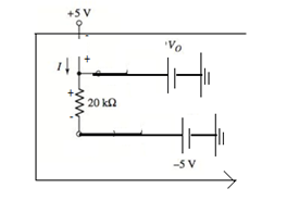
      MICROELECT. CIRCUIT ANALYSIS&DESIGN (LL), Chapter 1, Problem 1.47P , additional homework tip  23

      Vo+I(20k)+(5)=0Vo+0×(20k)+(5)=0Vo=5V

    For Vγ=0.6V

    The given circuit diagram is:

      MICROELECT. CIRCUIT ANALYSIS&DESIGN (LL), Chapter 1, Problem 1.47P , additional homework tip  24

    Assuming the diode is in OFF state. Hence, the modified circuit is:

      MICROELECT. CIRCUIT ANALYSIS&DESIGN (LL), Chapter 1, Problem 1.47P , additional homework tip  25

    From the circuit:

      VD<Vγ10V<0.6V

    In this circuit, the diode is reverse biased, so it is in OFF mode. Hence, the assumption is correct and the value of current I is zero.

    Applying Kirchhoff’s voltage law in the following circuit:
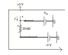
      MICROELECT. CIRCUIT ANALYSIS&DESIGN (LL), Chapter 1, Problem 1.47P , additional homework tip  26

      Vo+I(20k)+(5)=0Vo+0×(20k)+(5)=0Vo=5V

    Want to see more full solutions like this?

    Subscribe now to access step-by-step solutions to millions of textbook problems written by subject matter experts!
    Students have asked these similar questions
    complete the table in the attached photos. instructions are below the table
    Please show the solution and answers in each. Thank you. A 120 MVA, 19.5 kV generator has Xₛ = 1.5 pu and is connected to a transmission line by a transformer rated 150 MVA , 230 wye/18 delta kV Watts, and X = 0.1 pu. If the base to be used in the calculation is 100 MVA, 230 kV for the transmission line. a. Find the per-unit values to be used for the transformer and generator reactances. b. If the transformer delivers 80% of its rated capacity to the line at 220 kV, express the current in per unit. c. Find also the current in the genrator in amperes.
    I need an expert mathematical solution. The radiation intensity of an aperture antenna, mounted on an infinite ground plane with perpendicular to the aperture. is rotationally symmetric (not a function of 4), and it is given by U sin (77 sin 0) π sin Find the approximate directivity (dimensionless and in dB) using numerical integration. Use the DIRECTIVITY computer program at the end of this chapter.

    Chapter 1 Solutions

    MICROELECT. CIRCUIT ANALYSIS&DESIGN (LL)

    Ch. 1 - A silicon pn junction at T=300K is doped at...Ch. 1 - (a) A silicon pn junction at T=300K has a...Ch. 1 - (a) Determine Vbi for a silicon pn junction at...Ch. 1 - A silicon pn junction diode at T=300K has a...Ch. 1 - Recall that the forwardbias diode voltage...Ch. 1 - Consider the circuit in Figure 1.28. Let VPS=4V ,...Ch. 1 - (a) Consider the circuit shown in Figure 1.28. Let...Ch. 1 - The resistor parameter in the circuit shown in...Ch. 1 - Consider the diode and circuit in Exercise EX 1.8....Ch. 1 - Consider the circuit in Figure 1.28. Let R=4k and...Ch. 1 - The power supply (input) voltage in the circuit of...Ch. 1 - (a) The circuit and diode parameters for the...Ch. 1 - Determine the diffusion conductance of a pn...Ch. 1 - Determine the smallsignal diffusion resistance of...Ch. 1 - The diffusion resistance of a pn junction diode at...Ch. 1 - A pn junction diode and a Schottky diode both have...Ch. 1 - Consider the circuit shown in Figure 1.45....Ch. 1 - Consider the circuit shown in Figure 1.46. The...Ch. 1 - A Zener diode has an equivalent series resistance...Ch. 1 - The resistor in the circuit shown in Figure 1.45...Ch. 1 - Describe an intrinsic semiconductor material. What...Ch. 1 - Describe the concept of an electron and a hole as...Ch. 1 - Describe an extrinsic semiconductor material. What...Ch. 1 - Describe the concepts of drift current and...Ch. 1 - How is a pn junction formed? What is meant by a...Ch. 1 - How is a junction capacitance created in a...Ch. 1 - Write the ideal diode currentvoltage relationship....Ch. 1 - Describe the iteration method of analysis and when...Ch. 1 - Describe the piecewise linear model of a diode and...Ch. 1 - Define a load line in a simple diode circuit.Ch. 1 - Under what conditions is the smallsignal model of...Ch. 1 - Describe the operation of a simple solar cell...Ch. 1 - How do the i characteristics of a Schottky barrier...Ch. 1 - What characteristic of a Zener diode is used in...Ch. 1 - Describe the characteristics of a photodiode and a...Ch. 1 - (a) Calculate the intrinsic carrier concentration...Ch. 1 - (a) The intrinsic carrier concentration in silicon...Ch. 1 - Calculate the intrinsic carrier concentration in...Ch. 1 - (a) Find the concentration of electrons and holes...Ch. 1 - Gallium arsenide is doped with acceptor impurity...Ch. 1 - Silicon is doped with 51016 arsenic atoms/cm3 ....Ch. 1 - (a) Calculate the concentration of electrons and...Ch. 1 - A silicon sample is fabricated such that the hole...Ch. 1 - The electron concentration in silicon at T=300K is...Ch. 1 - (a) A silicon semiconductor material is to be...Ch. 1 - (a) The applied electric field in ptype silicon is...Ch. 1 - A drift current density of 120A/cm2 is established...Ch. 1 - An ntype silicon material has a resistivity of...Ch. 1 - (a) The applied conductivity of a silicon material...Ch. 1 - In GaAs, the mobilities are n=8500cm2/Vs and...Ch. 1 - The electron and hole concentrations in a sample...Ch. 1 - The hole concentration in silicon is given by...Ch. 1 - GaAs is doped to Na=1017cm3 . (a) Calculate no and...Ch. 1 - (a) Determine the builtin potential barrier Vbi in...Ch. 1 - Consider a silicon pn junction. The nregion is...Ch. 1 - The donor concentration in the nregion of a...Ch. 1 - Consider a uniformly doped GaAs pn junction with...Ch. 1 - The zerobiased junction capacitance of a silicon...Ch. 1 - The zerobias capacitance of a silicon pn junction...Ch. 1 - The doping concentrations in a silicon pn junction...Ch. 1 - (a) At what reversebias voltage does the...Ch. 1 - (a) The reversesaturation current of a pn junction...Ch. 1 - (a) The reversesaturation current of a pn junction...Ch. 1 - A silicon pn junction diode has an emission...Ch. 1 - Plot log10ID versus VD over the range 0.1VD0.7V...Ch. 1 - (a) Consider a silicon pn junction diode operating...Ch. 1 - A pn junction diode has IS=2nA . (a) Determine the...Ch. 1 - The reversebias saturation current for a set of...Ch. 1 - A germanium pn junction has a diode current of...Ch. 1 - (a)The reversesaturation current of a gallium...Ch. 1 - The reversesaturation current of a silicon pn...Ch. 1 - A silicon pn junction diode has an applied...Ch. 1 - A pn junction diode is in series with a 1M...Ch. 1 - Consider the diode circuit shown in Figure P1.39....Ch. 1 - The diode in the circuit shown in Figure P1.40 has...Ch. 1 - Prob. 1.41PCh. 1 - (a) The reversesaturation current of each diode in...Ch. 1 - (a) Consider the circuit shown in Figure P1.40....Ch. 1 - Consider the circuit shown in Figure P1.44....Ch. 1 - The cutin voltage of the diode shown in the...Ch. 1 - Find I and VO in each circuit shown in Figure...Ch. 1 - Repeat Problem 1.47 if the reversesaturation...Ch. 1 - (a) In the circuit Shown in Figure P1.49, find the...Ch. 1 - Assume each diode in the circuit shown in Figure...Ch. 1 - (a) Consider a pn junction diode biased at IDQ=1mA...Ch. 1 - Determine the smallsignal diffusion resistancefor...Ch. 1 - The diode in the circuit shown in Figure P1.53 is...Ch. 1 - The forwardbias currents in a pn junction diode...Ch. 1 - A pn junction diode and a Schottky diode have...Ch. 1 - The reversesaturation currents of a Schottky diode...Ch. 1 - Consider the Zener diode circuit shown in Figure...Ch. 1 - (a) The Zener diode in Figure P1.57 is ideal with...Ch. 1 - Consider the Zener diode circuit shown in Figure...Ch. 1 - The Output current of a pn junction diode used as...Ch. 1 - Using the currentvoltage characteristics of the...Ch. 1 - (a) Using the currentvoltage characteristics of...Ch. 1 - Use a computer simulation to generate the ideal...Ch. 1 - Use a computer simulation to find the diode...Ch. 1 - Design a diode circuit to produce the load line...Ch. 1 - Design a circuit to produce the characteristics...Ch. 1 - Design a circuit to produce the characteristics...Ch. 1 - Design a circuit to produce the characteristics...

    Additional Engineering Textbook Solutions

    Find more solutions based on key concepts
    Knowledge Booster
    Background pattern image
    Electrical Engineering
    Learn more about
    Need a deep-dive on the concept behind this application? Look no further. Learn more about this topic, electrical-engineering and related others by exploring similar questions and additional content below.
    Similar questions
    SEE MORE QUESTIONS
    Recommended textbooks for you
    Text book image
    Introductory Circuit Analysis (13th Edition)
    Electrical Engineering
    ISBN:9780133923605
    Author:Robert L. Boylestad
    Publisher:PEARSON
    Text book image
    Delmar's Standard Textbook Of Electricity
    Electrical Engineering
    ISBN:9781337900348
    Author:Stephen L. Herman
    Publisher:Cengage Learning
    Text book image
    Programmable Logic Controllers
    Electrical Engineering
    ISBN:9780073373843
    Author:Frank D. Petruzella
    Publisher:McGraw-Hill Education
    Text book image
    Fundamentals of Electric Circuits
    Electrical Engineering
    ISBN:9780078028229
    Author:Charles K Alexander, Matthew Sadiku
    Publisher:McGraw-Hill Education
    Text book image
    Electric Circuits. (11th Edition)
    Electrical Engineering
    ISBN:9780134746968
    Author:James W. Nilsson, Susan Riedel
    Publisher:PEARSON
    Text book image
    Engineering Electromagnetics
    Electrical Engineering
    ISBN:9780078028151
    Author:Hayt, William H. (william Hart), Jr, BUCK, John A.
    Publisher:Mcgraw-hill Education,
    [2015] Engineering Fundamentals 02: Unit systems. SI unit system [with closed caption]; Author: Yiheng Wang;https://www.youtube.com/watch?v=cryvZJ0KNqk;License: Standard YouTube License, CC-BY