Videos
Using Fig. 9.45, design a problem to help other students better understand admittance.
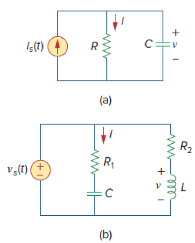
Figure 9.45
Design a problem to make better understand about the admittance using Figure 9.45.
Explanation of Solution
Problem design:
Determine the value of current
Formula used:
Write the expression to convert the time domain expression into phasor domain.
Here,
A is the magnitude,
t is the time, and
Write the expression to calculate the impedance of the passive elements resistor, inductor and capacitor.
Here,
Calculation:
(a)
The Figure 9.45(a) is redrawn as Figure 1 by assuming the values for the respective elements.
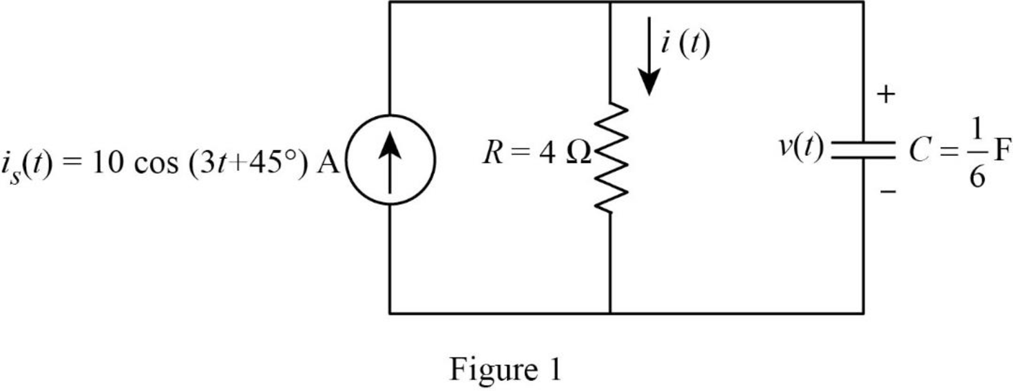
Refer to Figure 1, the current equation is,
Here, angular frequency
Use the equation (1) to express the above equation in phasor form.
Substitute
Substitute
The Figure 1 is redrawn as impedance circuit in the following Figure 2.
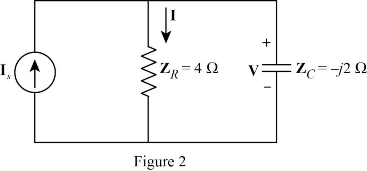
Apply current division rule on Figure 2 to find
Substitute
Use the equation (1) to express the above equation in time domain form.
Substitute
Refer to Figure 2, the voltage across the impedance
Substitute
Use the equation (1) to express the above equation in time domain form.
Substitute
Therefore, the value of current
(b)
The Figure 9.45(b) is redrawn as Figure 3 by assuming the values for the respective elements.
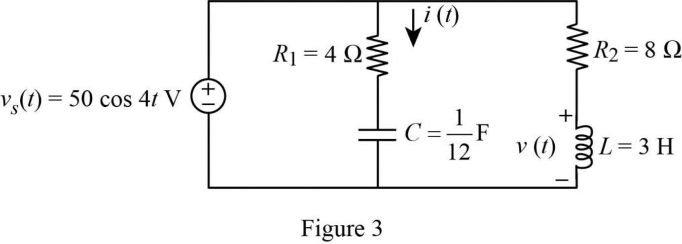
Refer to Figure 3, the voltage equation is,
Here, angular frequency
Use the equation (1) to express the above equation in phasor form.
Substitute
Substitute
Substitute
Substitute
The Figure 3 is redrawn as impedance circuit in the following Figure 4.
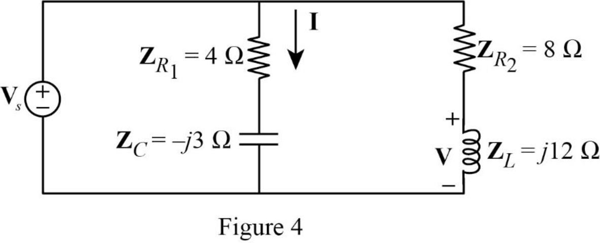
Refer to Figure 4, the impedances
Write the expression to calculate the equivalent impedance of the series connected impedances
Refer to Figure 4, the source voltage
Write the expression to calculate the current
Substitute
Substitute
Use the equation (1) to express the above equation in time domain form.
Substitute
Apply voltage division rule on Figure 4 to find
Substitute
Use the equation (1) to express the above equation in time domain form.
Substitute
Therefore, the value of current
Conclusion:
Thus, the problem to make better understand about the admittance using Figure 9.45 is designed.
Want to see more full solutions like this?
Chapter 9 Solutions
Fundamentals of Electric Circuits


- Q2 but when you get to part 3, can you please draw it outarrow_forwardplease solve manually. I need the drawing and the values too. Thank you!arrow_forwardTwo alternators, Y-connected 6.6 kV supply a load of 3000 kW at 0.8 p.f lagging. The synchronous mpedance of first alternator is (0.5+j10) Q/ph and second alternator is (0.4+j12) /ph. First alternator delivers 150 amp at 0.875 lag p.f. The two alterators are shared load equally. Determine the current, p.f., induced e.m.f, load angel, and maximum developed power of each alternator?arrow_forward
- A domestic load of 2300 kW at 0.88 p.f lagging and a motors load of 3400 kW at 0.85 p.f lagging are supplied by two alternators operating in parallel. If one alternator is delivering a load of 3300 kW at 0.9 p.f lagging, what will be the output power and p.f of the other alternator?arrow_forwardDetermine the value of Rr that necessary for the circuit in Fig.(2) to operate as an oscillator and then determine the frequency of oscillation. 0.001 F 0.001 F 0.001 F R₁ • 10 ΚΩ R₁ 10 k R • 10 ΚΩarrow_forward(a) For the circuit shown in Figure Q3(a) (RFC and Cc are forbias) (i) (ii) Draw the AC small signal equivalent circuit of the oscillator. From this equivalent circuit derive an equation for fo and the gain condition for the oscillations to start. VDD www RG eee RFC H Cc 北 5 C₁ L 000 C₂ Voarrow_forward
- Please solve this question step by step handwritten solution and do not use chat gpt or any ai toolsfor part ii) you may need to use nodal analysisarrow_forward12.1. Find the steady-state response vo (t) for the network. 00000- 1Ω ww 12 cos(t) V + www 202 1 H 202 1 F + 1Ω νο -arrow_forwardA Three-phase, 12 pole, Y-connected alternator has 108 slots and 14 conductors per slot. The windings are (5/6 th) pitched. The flux per pole is 57 mWb distributed sinusoidally over the pole. If the machine runs at 500 r.p.m., determine the following: (a) The frequency of the generated e.m.f., (b) The distribution factor, (c) The pitch factor, and (d) The phase and line values of the generated e.m.f.?arrow_forward
- Two 3-ph, 6.6 kV, Y-connected, alternators supply a load of 3000 kW at 0.8 p.f. lagging. The synchronou impedance per phase of machine A is (0.5+110) and that of machine B is (0.4 +J12) . The excitation of machine A adjusted so that it delivers 150 A. The load is shared equally between the machines. Determine the armature curre p.f., induced e.m.f., and load angle of each machine?arrow_forwardName the circuit below? The output voltage is initially zero and the pulse width is 200 μs. Find the Vout and draw the output waveform? +2.5 V V 247 -2.5 V C 0.01 F Ri W 10 ΚΩarrow_forwardPlease work outarrow_forward
 Introductory Circuit Analysis (13th Edition)Electrical EngineeringISBN:9780133923605Author:Robert L. BoylestadPublisher:PEARSON
 Delmar's Standard Textbook Of ElectricityElectrical EngineeringISBN:9781337900348Author:Stephen L. HermanPublisher:Cengage Learning
 Programmable Logic ControllersElectrical EngineeringISBN:9780073373843Author:Frank D. PetruzellaPublisher:McGraw-Hill Education
 Fundamentals of Electric CircuitsElectrical EngineeringISBN:9780078028229Author:Charles K Alexander, Matthew SadikuPublisher:McGraw-Hill Education
 Electric Circuits. (11th Edition)Electrical EngineeringISBN:9780134746968Author:James W. Nilsson, Susan RiedelPublisher:PEARSON
 Engineering ElectromagneticsElectrical EngineeringISBN:9780078028151Author:Hayt, William H. (william Hart), Jr, BUCK, John A.Publisher:Mcgraw-hill Education,