
Videos
A common-emitter equivalent circuit is shown in Figure P7.50. (a) What isthe expression for the Miller capacitance? (b) Derive the expression for thevoltage gain
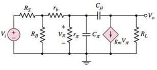
Figure P7.50
(a)
The expression for miller capacitance.
Answer to Problem 7.50P
The expression for miller capacitance is,
Explanation of Solution
Given:
The given circuit is shown below.

Calculation:
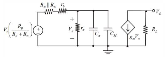
Draw the small signal equivalent circuit of figure including the equivalent miller capacitance

From figure, the thevenin voltage across the resistance
The equivalent thevenin resistance is,
From above figure, the expression for output voltage is,
Determine the expression for the Miller Capacitance.
Determine the expression for the Miller Capacitance.
Substitute
Thus, the expression for miller capacitance is,
(b)
The expression for voltage gain.
Answer to Problem 7.50P
The expression for voltage gain
Explanation of Solution
Given:
The given circuit is shown below.
Calculation:
Draw the small signal equivalent circuit of figure including the equivalent miller capacitance
In figure, the capacitors
The value of total capacitive reactance is,
Apply voltage division rule to write the expression for voltage
Derive the expression for voltage gain.
Further simplification as follows,
Consider
Therefore,
Thus, the expression for voltage gain is,
(c)
The expression for upper
Answer to Problem 7.50P
The expression for upper
Explanation of Solution
Given:
The given circuit is shown below.

Calculation:
The expression for voltage gain is,
From the voltage gain expression, the time constant is,
Determine the expression for upper
Substitute
Thus, the expression for upper
Want to see more full solutions like this?
Chapter 7 Solutions
Microelectronics: Circuit Analysis and Design


- Repairs have to be carried out on HV cir- cuit breaker No. 6 shown in Fig. 26. If the three 220 kV lines must be kept in service, which disconnecting switches must be kept open?arrow_forwardFind the voltage v(t) for t>=0 show all steps and redraw circuit as necessary, the switch closes at t=0 and v(t) is the voltage over the 4ohm resistor as shown in the circuit.arrow_forwardFind the voltage v(t) for t>=0 please redraw circuit as necessary and show all steps.arrow_forward
- Determine (a) the average and (b) rms values of the periodiccurrent waveform shown in Fig. P8.9arrow_forwardFind Eigenvalues and Eigenvectors for the following matrices: [5 -6 1 A = 1 1 0 3 0 1arrow_forwardUse Gauss-Jordan Elimination method to solve the following system: 4x1+5x2 + x3 = 2 x1-2x2-3x3 = 7 3x1 x2 2x3 = 1. -arrow_forward
- 3. As the audio frequency of Fig. 11-7 goes down, what components of Fig. 12-4 must be modified for normal operation? OD C₂ 100 HF R₁ 300 Re 300 ww 100A R 8 Voc Rz 10k reset output 3 R7 8 Voc 3 reset output Z discharge VR₁ 5k 2 trigger 2 trigger 7 discharge R 3 1k 5 control voltage threshold 6 5 control voltage 6 threshold GND Rs 2k C. C. 100 GND Uz LM555 1 Ce 0.01 U, LM555 0.01 8.01.4 PRO Fig. 11-7 Audio lutput Pulse width modulator R4 1k ww C7 Re 1k ww R7 100 VR 50k 10μ Ra R10 C₁. R1 3.9k 3.9k 0.14 100k TO w Rs 51 82 3 H 10 Carrier U₁ Ca Input A741 2.2 Us MC1496 PWM signal input R2 0.1100k Uz A741 41 Cs 1 Re 10k VR2 50k VR3 100k 14 12 C3. 3% + Ce 0.1 10μ 5 1A HH C +12V 0.1 O PWM Output C 0.02- R 100k +12 V Demodulated output 6 Ca 0.33 w R 10k R12 100k ww 31 о + 4A741 -12 V Fig. 12-4 PWM demodulator C 1500parrow_forwardDUC 1. In Fig. 12-4, what are the functions of the VR1 and VR2? 2. In Fig. 12-4, what is the function of the VR3? VR₁ 50k C₁ R1 0.1 100k Carrier Input U₁ A741 PWM signal input R41k www Re 1k w C7 ± 10μT R7 100 ww =L H C4 2.2 H W82 Rs 51 3 10 U3 MC1496 C2 R2 U2 A741 22 0.1 100k VR2 50k VR3 100kr 14 C3 10μ 1k 0.1 4 5 6 12 m Re 10k R9 R102 3.9k 3.9k HHI C10 0.1 -0 +12V C11 R 0.02 100k +12 V Demodulated output C R11 R12 A741 0.33 10k 100k -12 V Ca 1μ C12 1500p PRODUC Fig. 12-4 PWM demodulator PRODUCTSarrow_forward10.37 Use mesh analysis to find currents I₁, I2, and I3 in the circuit of Fig. 10.82. ML 120-90° V 120 -30° V Figure 10.82 For Prob. 10.37. N N Z=80-135arrow_forward
- 3. Find the phasor current I。 in the circuit shown below. Be aware of the direction markings. (15 pts) 1052 I 5057 ①520 Amps 2012 j5052arrow_forward10.93 Figure 10.135 shows a Colpitts oscillator. Show that the ed oscillation frequency is 1 fo= 2π √√LCT where CTC₁C2/(C₁ + C₂). Assume R; >>> R₁ + Rf ww Vo L m C₂ C₁ 5 Xci Figure 10.135 A Colpitts oscillator; for Prob. 10.93. (Hint: Set the imaginary part of the impedance in the feedback circuit equal to zero.)arrow_forwardDetermine (a) the average and (b) rms values of the periodiccurrent waveform shown in Fig. P8.3.arrow_forward
 Introductory Circuit Analysis (13th Edition)Electrical EngineeringISBN:9780133923605Author:Robert L. BoylestadPublisher:PEARSON
 Delmar's Standard Textbook Of ElectricityElectrical EngineeringISBN:9781337900348Author:Stephen L. HermanPublisher:Cengage Learning
 Programmable Logic ControllersElectrical EngineeringISBN:9780073373843Author:Frank D. PetruzellaPublisher:McGraw-Hill Education
 Fundamentals of Electric CircuitsElectrical EngineeringISBN:9780078028229Author:Charles K Alexander, Matthew SadikuPublisher:McGraw-Hill Education
 Electric Circuits. (11th Edition)Electrical EngineeringISBN:9780134746968Author:James W. Nilsson, Susan RiedelPublisher:PEARSON
 Engineering ElectromagneticsElectrical EngineeringISBN:9780078028151Author:Hayt, William H. (william Hart), Jr, BUCK, John A.Publisher:Mcgraw-hill Education,