
Videos
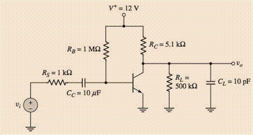
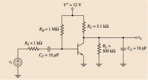
The parameters of the transistor in the circuit in Figure P7.40 are
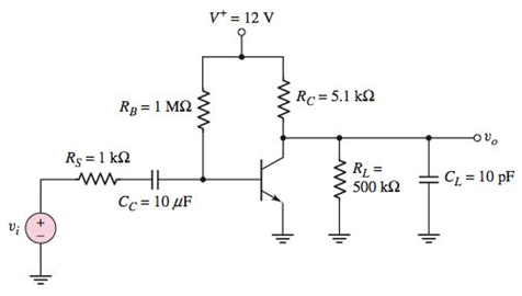 Figure P7.40
a.
To draw: Three equivalent circuits that represent the amplifier in the low frequency range, mid-band range and the high frequency range.
Answer to Problem 7.40P
Three equivalent circuits that represent the amplifier in the low frequency range, mid-band range and the high frequency range are shown in Figure 1, 2 and 3 respectively.
Explanation of Solution
Given:
The diagram is given as:
Calculation:
Calculate the value of current
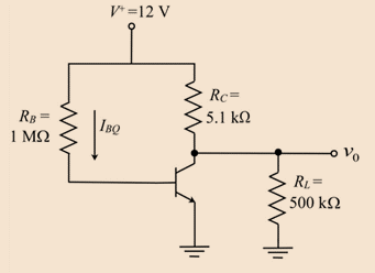
Applying Kirchhoff s voltage law in the above loop:
Here,
Substituting
The quiescent collector current
Here,
Substituting
Evaluating the resistance
Here,
Evaluating the transconductance
Substituting
Figure 2 shows the low −frequency small signal transistor with the output resistance
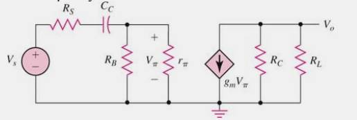
Figure 1
In the mid-frequency range, the coupling and bypass capacitors are short-circuited and the load capacitors are open-circuited.
It shows the mid-frequency small signal transistor with the output resistance
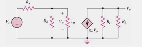
Figure 2
In the high-frequency range, the coupling and bypass capacitors are short-circuited and the load capacitors are included.
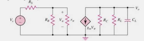
Figure 3
Hence, the three equivalent circuits that represent the amplifier in the low-frequency range, mid-band range, and high-frequency range are plotted.
b.
To sketch: The bode magnitude plot.
Answer to Problem 7.40P
The sketch of bode magnitude plot is shown in Figure 4.
Explanation of Solution
Given:
The diagram is given as:
Calculation:
Consider the values, calculated in part (a).
The effect of the coupling capacitor
The figure shows the bode plot for the circuit having a combination of a coupling capacitor and load capacitor:
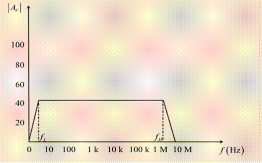
Figure 4
Hence, the bode magnitude plot is sketched.
c.
The values of the
Answer to Problem 7.40P
The values are:
Explanation of Solution
Given:
The diagram is given as:
Calculation:
Evaluating the midband gain by short-circuiting the coupling and bypass capacitors and open-circuiting the load capacitors.
Substituting the values,
Evaluating the gain in dB:
Substituting
Hence, the value of gain
Evaluating the equivalent resistance
Substituting
Evaluating the time constant
Substituting
Evaluating the equivalent resistance
Substituting
Evaluating the time constant
Substituting
Evaluate the lower corner frequency
Substituting
Evaluated the upper corner frequency:
Substitute
Want to see more full solutions like this?
Chapter 7 Solutions
Microelectronics: Circuit Analysis and Design
Additional Engineering Textbook Solutions
Elementary Surveying: An Introduction To Geomatics (15th Edition)
Degarmo's Materials And Processes In Manufacturing
Database Concepts (8th Edition)
Electric Circuits. (11th Edition)
SURVEY OF OPERATING SYSTEMS
Vector Mechanics for Engineers: Statics and Dynamics


- Consider the following 4×1 multiplexer with inputs: w0=2, w1=1, w2=x2' and w3=0 And with switches: S1 x1 and S0=x0 What is the multiplexer output f as a function of x2, x1 and x0?arrow_forwardI need help adding a capacitor and a Zener diode to my circuit. I’m looking for a simple sketch or diagram showing how to connect them. i want diagram with final circuit after adding the zener diad and capacitor. don't do calclution or anything. thanksarrow_forwardQuestion 3 AC Motor Drives [15]Calculate the instantaneous currents delivered by the inverter if the direct axiscurrent required at a particular instant is 8.66A and the quadrature current is5A. Derive all equations for the three currents.arrow_forward
- A certain signal f(t) has the following PSD (assume 12 load): Sp (w) = new + 8(w) - 1.5) + (w + 1.5)] (a) What is the mean power in the bandwidth w≤2 rad/see? (b) What is the mean power in the bandwidth -1.9 to 0.99 rad/sec? Paress(w) dw 2ㅈ -arrow_forward(75 Marks) JA signal (t) is bond 7)(t)(t) and f(t), are band-limited to 1.2 kHz each. These signals are to be limited to 9.6 kHz, and three other signals transmitted by means of time-division multiplexing. Set up scheme for accomplishing this multiplexing requirement, with each signal sampled at its Nyquist rate. What must be the speed of the commutator (the output but ram-k bit/sec)? the minimum band width? (25 Marks)arrow_forwardDraw the digital modulation outputs, ASK Amplitude Shift Keying) FSK (Frequency Shift Keying) and PSK (Phase Shift Keying). For baseband and carriet frequency as shown 101 wwwwwwwwwwww 010 BASESAND basband CARRIER Carralarrow_forward
- please show full working. I've included the solutionarrow_forwardcan you please show working and steps. The answer is 8kohms.arrow_forwardPSD A certain signal f(t) has the following PSD (assume 12 load): | Sƒ(w) = π[e¯\w\ + 8(w − 2) + +8(w + 2)] (a) What is the mean power in the bandwidth w≤ 1 rad/sec? (b) What is the mean power in the bandwidth 0.99 to 1.01 rad/sec? (c) What is the mean power in the bandwidth 1.99 to 2.01 rad/sec? (d) What is the total mean power in (t)? Pav= + 2T SfLw) dw - SALW)arrow_forward
- An AM modulation waveform signal:- p(t)=(8+4 cos 1000πt + 4 cos 2000πt) cos 10000nt (a) Sketch the amplitude spectrum of p(t). (b) Find total power, sideband power and power efficiency. (c) Find the average power containing of each sideband.arrow_forwardCan you rewrite the solution because it is unclear? AM (+) = 8(1+ 0.5 cos 1000kt +0.5 ros 2000ks) = cos 10000 πt. 8 cos wat + 4 cos wit + 4 cos Wat coswet. -Jet jooort J11000 t = 4 e jqooort jgoort +4e + e +e j 12000rt. 12000 kt + e +e jooxt igoo t te (w) = 8ES(W- 100007) + 8IS (W-10000) USBarrow_forwardCan you rewrite the solution because it is unclear? AM (+) = 8(1+0.5 cos 1000kt +0.5 ros 2000 thts) = cos 10000 πt. 8 cos wat + 4 cos wit + 4 cos Wat coswet. J4000 t j11000rt $14+) = 45 jqooort +4e + e + e j 12000rt. 12000 kt + e +e +e Le jsoort -; goon t te +e Dcw> = 885(W- 100007) + 8 IS (W-10000) - USBarrow_forward
 Introductory Circuit Analysis (13th Edition)Electrical EngineeringISBN:9780133923605Author:Robert L. BoylestadPublisher:PEARSON
 Delmar's Standard Textbook Of ElectricityElectrical EngineeringISBN:9781337900348Author:Stephen L. HermanPublisher:Cengage Learning
 Programmable Logic ControllersElectrical EngineeringISBN:9780073373843Author:Frank D. PetruzellaPublisher:McGraw-Hill Education
 Fundamentals of Electric CircuitsElectrical EngineeringISBN:9780078028229Author:Charles K Alexander, Matthew SadikuPublisher:McGraw-Hill Education
 Electric Circuits. (11th Edition)Electrical EngineeringISBN:9780134746968Author:James W. Nilsson, Susan RiedelPublisher:PEARSON
 Engineering ElectromagneticsElectrical EngineeringISBN:9780078028151Author:Hayt, William H. (william Hart), Jr, BUCK, John A.Publisher:Mcgraw-hill Education,