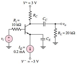
Consider the circuit shown in Figure P7.32. The transistor parameters are

Figure P7.32
(a)
The value of
Answer to Problem 7.32P
The value of collector resistor,
Explanation of Solution
Given:
The given circuit is shown below.

Calculation:
From figure, the value of emitter current is,
The value of base current is,
Substitute
The value of collector current is,
Substitute
The value of emitter voltage is,
Substitute
The value of collector voltage is,
Substitute
The value of collector resistor is,
Substitute 3 V for
(b)
The mid band gain
Answer to Problem 7.32P
The value of mid-band gain
Explanation of Solution
Given:
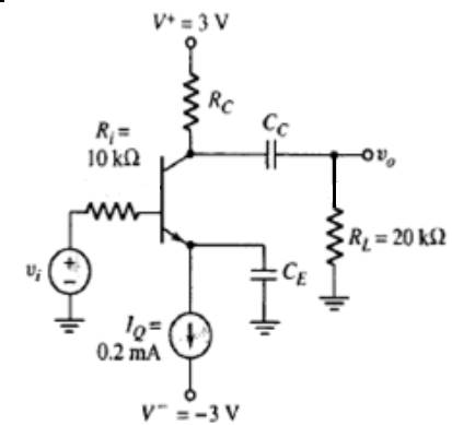
The given circuit is shown below.

Calculation:
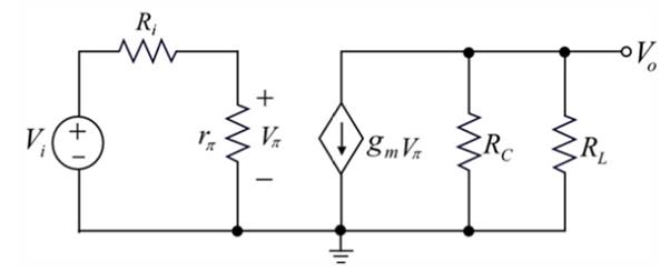
Draw the small signal equivalent circuit of figure to derive expression for mid band gain.

Apply voltage division rule to calculate the voltage across the base input resistor associated withthe input portion of the circuit.
Apply Kirchhoff's current law at output node in Figure 1
Substitute
The value of base input resistance.
Substitute
The value of transconductance is,
Substitute
The value of mid-band gain is,
Substitute
for
(c)
To derive: The expression for the corner frequencies associated with
Answer to Problem 7.32P
The expression for the corner frequency associated with
The expression for the corner frequency associated with
Explanation of Solution
Given:
The given circuit is shown below.

Calculation:
Derive the expression for the comer frequency associated with
Thus, the expression for the corner frequency associated with
Derive the expression for the comer frequency associated with
Thus, the expression for the corner frequency associated with
(d)
The value of
Answer to Problem 7.32P
The value of capacitance,
The value of capacitance,
Explanation of Solution
Given:
The given circuit is shown below.

Calculation:
Determine the value of capacitance,
Substitute
Thus, the value of capacitance,
Determine the value of capacitance,
Substitute
Thus, the value of capacitance,
Want to see more full solutions like this?
Chapter 7 Solutions
Microelectronics: Circuit Analysis and Design
- A certain magnetic circuit may be regarded as consisting of three parts, A, B and C in series, each one of which has a uniform cross-sectional area. Part A has a length of 300 mm and a cross- sectional area of 450 mm². Part B has a length of 120 mm and a cross-sectional area of 300 mm². Part C is an airgap 1.0 mm in length and of cross-sectional area 350 mm². The flux in the airgap is 0.35 mWb. Neglect magnetic leakage and fringing. The magnetic characteristic for parts A and B is given by: H (A/m) 400 560 800 1280 1800 B (T) 0.7 0.85 1.0 1.15 1.25 Calculate: i. The reluctance of each part, that is, of Part A, Part B, and Part C ii. The total reluctance of the magnetic circuit. iii. The total m.m.f.arrow_forwardHW_02.pdf EE 213-01 Assignments HW_#2 Toms are as muIcate uah.instructure.com b Answered: HW_#1 HW_01.pdf EE 213-01 Assignments P Pearson MyLab and Mastering uah.instructure.com P Course Home Watc... ✓ Download → Info × Close 1) (5 pts)For the circuit shown, find the value of Ia, Ib, Ic and Va: Ib 10 Ohms + Ic 40 Ohms 20 Ohms 70 Volts a Page 1 > of 2 - ZOOM + pui via Canvas Hint: use KCL to find Ic in terms of la and lb, use KVL around the right loop to find a relationship between la and lb, use KVL around the outer loop to solve for a current value (use ohms law for the voltage drops across the resistors) 2) (5 pts) – For problem 1, show that the power supplied (delivered) by the source equals the power absorbed by the resistors. 3) (5 pts) Determine the equivalent resistance looking into terminals a-b for the two circuits shown. Use series and parallel resistor combinations. Hint: work from the opposite end of terminals a-b towards terminals a-b a) 24 Ohms 10 Ohms 8 Ohms G a REQ b)…arrow_forwardA three-phase load consists of three identical impedances connected in delta. The impedances have a value of (100 + j40) Q. The supply voltage is 440 V. The two- wattmeter method is used to determine the total power drawn by the load. One wattmeter, W₁, has its current coil connected in the blue line and its voltage coil connected between the yellow and blue lines. Calculate: a) The power measured by each wattmeter b) The power factor of the load using the wattmeter readings c) The apparent power supplied to the load d) The reactive power drawn by the load.arrow_forward
- 4- A 75 KW, 250 V shunt generator has R₁ = 0.03 2 and RF =50 2. The generator has 6 poles and is lap wound with totally 400 conductors. The generator runs at 600 rpm on full load. The bore of the machine is 42 cm (in diameter), its axial length is 28 cm and each pole subtends an angle of 54 °. Field pole a) b) c) Find the airgap flux density. (10 pt) Find the induced voltage under full load. (10 pt) Find the average number of active conductors. (5 pts) 28 cm 21 cm 60° Armaturearrow_forwarda) The phase currents in a delta - connected three-phase load are as follows: between the red and yellow lines, 60 A at p.f. 0.9 leading; between the yellow and blue lines, 40 A at 0.95 p.f lagging; between the blue and red lines, 50 A at p.f. 0.8 lagging. The supply voltage is 240 V. Draw a labeled diagram of the circuit and calculate the line currents. Note: Use VRY as the reference phasor. b) The two-wattmeter method is used to measure the total power drawn by the load in 1 (a) above. Wattmeter one has its current coil connected in the yellow line and its voltage coil connected between the yellow and red lines. Calculate: i. The power measured by each wattmeter. ii. The power factor of the load.arrow_forwardQUESTION NO. 1 a) State Lenz Law b) Explain Flux density c) A wire, 100 mm long, is moved at a uniform speed of 4 m/s at right angles to its length and to a uniform magnetic field. Calculate the density of the field if the e.m.f. generated in the wire is 0.15 V. If the wire forms part of a closed circuit having a total resistance of 0.04 2, calculate the force on the wire in newtons.arrow_forward
- In Figure (a) the drawing of the bipolar circuit was as shown in Figure 4. Draw me a unipolar circuit and how it will be in Figure (b). Please draw the circuit with the transistors.arrow_forwardSOLVE ON PAPER NOT BY CHATGPTarrow_forwardDraw fabrication layer transistor MS (schottky diode)arrow_forward
- Need Handwritten solution not using chatgt or AIarrow_forward2. Suppose G₁(s) = (s+2) G₂(s) = (s-3) C(s) Find the transfer function G(s): for each of the following three configurations R(s) shown in Figure 1. Note (a) is a cascaded (series) system, (b) is a parallel system, and (c) is a feedback (closed-loop) system. € (c) C(s) R(s) G₁(s) G2(5) G₁(s) R(s) C(s) G2(s) C(s) R(s) G₁(s) G₂(s) Figure 1arrow_forwardDetermine the transformer's active power losses and primary voltage (Figure 1). The busbar's voltage at the transformer's secondary side is 20.5 kV. Load P is 6 MW, and the power factor is 0.95ind.arrow_forward
 Introductory Circuit Analysis (13th Edition)Electrical EngineeringISBN:9780133923605Author:Robert L. BoylestadPublisher:PEARSON
 Delmar's Standard Textbook Of ElectricityElectrical EngineeringISBN:9781337900348Author:Stephen L. HermanPublisher:Cengage Learning
 Programmable Logic ControllersElectrical EngineeringISBN:9780073373843Author:Frank D. PetruzellaPublisher:McGraw-Hill Education
 Fundamentals of Electric CircuitsElectrical EngineeringISBN:9780078028229Author:Charles K Alexander, Matthew SadikuPublisher:McGraw-Hill Education
 Electric Circuits. (11th Edition)Electrical EngineeringISBN:9780134746968Author:James W. Nilsson, Susan RiedelPublisher:PEARSON
 Engineering ElectromagneticsElectrical EngineeringISBN:9780078028151Author:Hayt, William H. (william Hart), Jr, BUCK, John A.Publisher:Mcgraw-hill Education,


