Fundamentals of Electric Circuits
6th Edition
ISBN: 9780078028229
Author: Charles K Alexander, Matthew Sadiku
Publisher: McGraw-Hill Education
expand_more
expand_more
format_list_bulleted
Concept explainers
Videos
Textbook Question
Chapter 5, Problem 57P
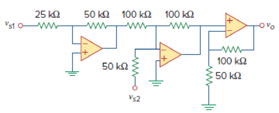
Find vo in the op amp circuit of Fig. 5.84.
Expert Solution & Answer
Want to see the full answer?
Check out a sample textbook solution
Students have asked these similar questions
Write the angle expression form of first null beam width FNBW) for 2/2 dipole.
for 즐, 꽃
3
The circuit is in the DC steady state,
So all transients are passed. What are the
values of 1 and V, under those conditions.
P
24v
+
+ √2
АЛАД
42
4F
3.H
ww
22
eee
+
203
V
Find the value of Vc (t) for all I
That is, the complete response including
natural and forced responses.)
АДДА
422
OV
ДААД
t = 0
3F
+
V(t)
-
Chapter 5 Solutions
Fundamentals of Electric Circuits
Ch. 5.2 - If the same 741 op amp in Example 5.1 is used in...Ch. 5.3 - Repeat Example 5.1 using the ideal op amp model....Ch. 5.4 - Practice Problem 5.3 Figure 5.13 For Practice...Ch. 5.4 - Two kinds of current-to-voltage converters (also...Ch. 5.5 - Calculate vo in the circuit of Fig. 5.20. Answer:...Ch. 5.6 - Practice Problem 5.6 Find vo and io in the op amp...Ch. 5.7 - Design a difference amplifier with gain 7.5....Ch. 5.7 - Obtain io in the instrumentation amplifier circuit...Ch. 5.8 - Practice Problem 5.9 Figure 5.30 For Practice...Ch. 5.8 - If v1 = 5 V and v2 = 5 V, find vo in the op amp...
Ch. 5.9 - Rework Practice Prob. 5.1 using PSpice. If the...Ch. 5.10 - A three-bit DAC is shown in Fig. 5.37. (a)...Ch. 5.10 - Determine the value of the external gain-setting...Ch. 5 - The two input terminals of an op amp are labeled...Ch. 5 - For an ideal op amp, which of the following...Ch. 5 - For the circuit in Fig. 5.40, voltage vo is: (a)6...Ch. 5 - For the circuit in Fig. 5.40, current ix is:...Ch. 5 - If vs = 0 in the circuit of Fig. 5.41, current io...Ch. 5 - If vs = 8 mV in the circuit of Fig. 5.41, the...Ch. 5 - Refer to Fig. 5.41. If vs = 8 mV, voltage va is:...Ch. 5 - The power absorbed by the 4-k resistor in Fig....Ch. 5 - Which of these amplifiers is used in a...Ch. 5 - Difference amplifiers are used in (please check...Ch. 5 - The equivalent model of a certain op amp is shown...Ch. 5 - The open-loop gain of an op amp is 50,000....Ch. 5 - Determine the voltage input to the inverting...Ch. 5 - The output voltage of an op amp is 4 V when the...Ch. 5 - For the op amp circuit of Fig. 5.44, the op amp...Ch. 5 - Using the same parameters for the 741 op amp in...Ch. 5 - 5.7 The op amp in Fig. 5.46 has Ri = 100 k, Ro =...Ch. 5 - Obtain vo for each of the op amp circuits in Fig....Ch. 5 - Determine vo for each of the op amp circuits in...Ch. 5 - Prob. 10PCh. 5 - Using Fig. 5.50, design a problem to help other...Ch. 5 - Calculate the voltage ratio vo/vs for the op amp...Ch. 5 - Find vo and io in the circuit of Fig. 5.52. Figure...Ch. 5 - Determine the output voltage vo in the circuit of...Ch. 5 - (a)Determine the ratio vo/is in the op amp circuit...Ch. 5 - Using Fig. 5.55, design a problem to help students...Ch. 5 - Prob. 17PCh. 5 - For the circuit shown in Figure 5.57, solve for...Ch. 5 - Determine io in the circuit of Fig. 5.58. Figure...Ch. 5 - In the circuit of Fig. 5.59, calculate vo of vs =...Ch. 5 - Calculate vo in the op amp circuit of Fig. 5.60....Ch. 5 - Design an inverting amplifier with a gain of 15.Ch. 5 - For the op amp circuit in Fig. 5.61, find the...Ch. 5 - In the circuit shown in Fig. 5.62, find k in the...Ch. 5 - Calculate vo in the op amp circuit of Fig. 5.63....Ch. 5 - Using Fig. 5.64, design a problem to help other...Ch. 5 - Find vo in the op amp circuit of Fig. 5.65. Figure...Ch. 5 - Prob. 28PCh. 5 - Determine the voltage gain vo/vi of the op amp...Ch. 5 - In the circuit shown in Fig. 5.68, find ix and the...Ch. 5 - For the circuit in Fig. 5.69, find ix. Figure 5.69...Ch. 5 - Calculate ix and vo in the circuit of Fig. 5.70....Ch. 5 - Refer to the op amp circuit in Fig. 5.71....Ch. 5 - Given the op amp circuit shown in Fig. 5.72,...Ch. 5 - Design a noninverting amplifier with a gain of...Ch. 5 - For the circuit shown in Fig. 5.73, find the...Ch. 5 - Determine the output of the summing amplifier in...Ch. 5 - Using Fig. 5.75, design a problem to help other...Ch. 5 - For the op amp circuit in Fig. 5.76, determine the...Ch. 5 - Referring to the circuit shown in Fig. 5.77,...Ch. 5 - An averaging amplifier is a summer that provides...Ch. 5 - The feedback resistor of a three-input averaging...Ch. 5 - The feedback resistor of a five-input averaging...Ch. 5 - Show that the output voltage vo of the circuit in...Ch. 5 - Design an op amp circuit to perform the following...Ch. 5 - Using only two op amps, design a circuit to solve...Ch. 5 - The circuit in Fig. 5.79 is for a difference...Ch. 5 - The circuit in Fig. 5.80 is a differential...Ch. 5 - Design a difference amplifier to have a gain of 4...Ch. 5 - Design a circuit to amplify the difference between...Ch. 5 - Using two op amps, design a subtractor.Ch. 5 - Design an op amp circuit such that vo = 4v1 + 6v2 ...Ch. 5 - The ordinary difference amplifier for fixed-gain...Ch. 5 - Determine the voltage transfer ratio vovs in the...Ch. 5 - In a certain electronic device, a three-stage...Ch. 5 - Using Fig. 5.83, design a problem to help other...Ch. 5 - Find vo in the op amp circuit of Fig. 5.84.Ch. 5 - Calculate io in the op amp circuit of Fig. 5.85....Ch. 5 - In the op amp circuit of Fig. 5.86, determine the...Ch. 5 - Calculate vo/vi in the op amp circuit of Fig....Ch. 5 - Determine vo in the circuit of Fig. 5.88. Figure...Ch. 5 - Obtain the closed-loop voltage gain vo/vi of the...Ch. 5 - Determine the gain vovi of the circuit in Fig....Ch. 5 - For the op amp circuit shown in Fig. 5.91, find...Ch. 5 - Find vo in the op amp circuit of Fig. 5.92.Ch. 5 - For the circuit in Fig. 5.93, find vo.Ch. 5 - Obtain the output vo in the circuit of Fig. 5.94....Ch. 5 - Find vo in the circuit of Fig. 5.95, assuming that...Ch. 5 - Find vo in the circuit of Fig. 5.95, assuming that...Ch. 5 - Determine vo in the op amp circuit of Fig. 5.96.Ch. 5 - Determine vo in the op amp circuit of Fig. 5.97.Ch. 5 - Find the load voltage vL in the circuit of Fig....Ch. 5 - Determine the load voltage vL in the circuit of...Ch. 5 - Find io in the op amp circuit of Fig. 5.100....Ch. 5 - Rework Example 5.11 using the nonideal op amp...Ch. 5 - Solve Prob. 5.19 using PSpice or MultiSim and op...Ch. 5 - Solve Prob. 5.48 using PSpice or MultiSim and op...Ch. 5 - Use PSpice or MultiSim to obtain vo in the circuit...Ch. 5 - Determine vo in the op amp circuit of Fig. 5.102,...Ch. 5 - Use PSpice or MultiSim to solve Prob. 5.70....Ch. 5 - Use PSpice or MultiSim to verify the results in...Ch. 5 - Prob. 82PCh. 5 - Design a six-bit digital-to-analog converter. (a)...Ch. 5 - A four-bit R-2R ladder DAC is presented in Fig....Ch. 5 - In the op amp circuit of Fig. 5.104, find the...Ch. 5 - Design a voltage controlled ideal current source...Ch. 5 - Figure 5.105 displays a two-op-amp instrumentation...Ch. 5 - Figure 5.106 shows an instrumentation amplifier...Ch. 5 - Design a circuit that provides a relationship...Ch. 5 - The op amp circuit in Fig. 5.107 is a current...Ch. 5 - A noninverting current amplifier is portrayed in...Ch. 5 - Refer to the bridge amplifier shown in Fig. 5.109....Ch. 5 - A voltage-to-current converter is shown in Fig....
Knowledge Booster


Learn more about
Need a deep-dive on the concept behind this application? Look no further. Learn more about this topic, electrical-engineering and related others by exploring similar questions and additional content below.Similar questions
- 1.0 Half-power point (left) 0.5 Minor lobes Main lobe maximum direction Main lobe Half-power point (right) Half-power beamwidth (HP) Beamwidth between first nulls (BWFN) *Which of the following Lobes of an antenna Pattern 180 out of Phase the main Lobe ? And where are the ch other gems ?arrow_forwardThe normalized radiation intensity of an antenna is represented by U(0) = cos² (0) cos² (30), w/sr Find the a. half-power beamwidth HPBW (in radians and degrees) b. first-null beamwidth FNBW (in radians and degrees)arrow_forwardQ1/ Route the following flood hydrograph through a river reach for which storage duration constant = 10 hr and weighted factor = 0.25. At the start of the inflow flood, the outflow discharge is 60m³/s. Inflow (m/s) Time (hr) 140 60 100 0 4 8 12 16 120 80 40 20 Q2/ Answer the following: 1. Define water requirements and list the losses of irrigation. Q3/ Irrigation project with the following data: = 150 mm/m Root Zone Depth (RZD) = 1.1 m 15% of the net depth - Available Water PAD = 50%, Leaching Requirement Rainfall = 12 mm, = water Losses = 10% of the net depth. If the net water depth added after depletion of already available water, Calculate: gross irrigation water, and application efficiency. C= Carrow_forward
- A3 m long cantilever ABC is built-in at A, partially supported at B, 2 m from A, with a force of 10 kN and carries a vertical load of 20 kN at C. A uniformly distributed bad of 5 kN/m is also applied between A and B. Determine (a) the values of the vertical reaction and built-in moment at A and (b) the deflection of the free end C of the cantilever, Develop an expression for the slope of the beam at any position and hence plot a slope diagram. E = 208GN / (m ^ 2) and 1 = 24 * 10 ^ - 6 * m ^ 4arrow_forward7. Consider the following feedback system with a proportional controller. K G(s) The plant transfer function is given by G(s) = 10 (s + 2)(s + 10) You want the system to have a damping ratio of 0.3 for unit step response. What is the value of K you need to choose to achieve the desired damping ratio? For that value of K, find the steady-state error for ramp input and settling time for step input. Hint: Sketch the root locus and find the point in the root locus that intersects with z = 0.3 line.arrow_forwardCreate the PLC ladder logic diagram for the logic gate circuit displayed in Figure 7-35. The pilot light red (PLTR) output section has three inputs: PBR, PBG, and SW. Pushbutton red (PBR) and pushbutton green (PBG) are inputs to an XOR logic gate. The output of the XOR logic gate and the inverted switch SW) are inputs to a two-input AND logic gate. These inputs generate the pilot light red (PLTR) output. The two-input AND logic gate output is also fed into a two-input NAND logic PBR PBG SW TSW PLTR Figure 7-35. Logic gate circuit for Example 7-3. PLTW Goodheart-Willcox Publisher gate. The temperature switch (TSW) is the other input to the NAND logic gate. The output generated from the NAND logic gate is labeled pilot light white (PLTW).arrow_forward
- Imaginary Axis (seconds) 1 6. Root locus for a closed-loop system with L(s) = is shown below. s(s+4)(s+6) 15 10- 0.89 0.95 0.988 0.988 -10 0.95 -15 -25 0.89 20 Root Locus 0.81 0.7 0.56 0.38 0.2 5 10 15 System: sys Gain: 239 Pole: -0.00417 +4.89 Damping: 0.000854 Overshoot (%): 99.7 Frequency (rad/s): 4.89 System: sys Gain: 16.9 Pole: -1.57 Damping: 1 Overshoot (%): 0 Frequency (rad/s): 1.57 0.81 0.7 0.56 0.38 0.2 -20 -15 -10 -5 5 10 Real Axis (seconds) From the values shown in the figure, compute the following. a) Range of K for which the closed-loop system is stable. b) Range of K for which the closed-loop step response will not have any overshoot. Note that when all poles are real, the step response has no overshoot. c) Smallest possible peak time of the system. Note that peak time is the smallest when wa is the largest for the dominant pole. d) Smallest possible settling time of the system. Note that peak time is the smallest when σ is the largest for the dominant pole.arrow_forwardFor a band-rejection filter, the response drops below this half power point at two locations as visualised in Figure 7, we need to find these frequencies. Let's call the lower frequency-3dB point as fr and the higher frequency -3dB point fH. We can then find out the bandwidth as f=fHfL, as illustrated in Figure 7. 0dB Af -3 dB Figure 7. Band reject filter response diagram Considering your AC simulation frequency response and referring to Figure 7, measure the following from your AC simulation. 1% accuracy: (a) Upper-3db Frequency (fH) = Hz (b) Lower-3db Frequency (fL) = Hz (c) Bandwidth (Aƒ) = Hz (d) Quality Factor (Q) =arrow_forwardP 4.4-21 Determine the values of the node voltages V1, V2, and v3 for the circuit shown in Figure P 4.4-21. 29 ww 12 V +51 Aia ww 22. +21 ΖΩ www ΖΩ w +371 ①1 1 Aarrow_forward
- 1. What is the theoretical attenuation of the output voltage at the resonant frequency? Answer to within 1%, or enter 0, or infinity (as “inf”) Attenuation =arrow_forwardWhat is the settling time for your output signal (BRF_OUT)? For this question, We define the settling time as the period of time it has taken for the output to settle into a steady state - ie when your oscillation first decays (aka reduces) to less than approximately 1/20 (5%) of the initial value. (a) Settling time = 22 μs Your last answer was interpreted as follows: Incorrect answer. Check 22 222 What is the peak to peak output voltage (BRF_OUT pp) at the steady state condition? You may need to use the zoom function to perform this calculation. Select a time point that is two times the settling time you answered in the question above. Answer to within 10% accuracy. (a) BRF_OUT pp= mVpp As you may have noticed, the output voltage amplitude is a tiny fraction of the input voltage, i.e. it has been significantly attenuated. Calculate the attenuation (decibels = dB) in the output signal as compared to the input based on the formula given below. Answer to within 1% accuracy.…arrow_forwardmy previous answers for a,b,d were wrong a = 1050 b = 950 d=9.99 c was the only correct value i got previously c = 100hz is correctarrow_forward
arrow_back_ios
SEE MORE QUESTIONS
arrow_forward_ios
Recommended textbooks for you
 Introductory Circuit Analysis (13th Edition)Electrical EngineeringISBN:9780133923605Author:Robert L. BoylestadPublisher:PEARSON
 Delmar's Standard Textbook Of ElectricityElectrical EngineeringISBN:9781337900348Author:Stephen L. HermanPublisher:Cengage Learning
 Programmable Logic ControllersElectrical EngineeringISBN:9780073373843Author:Frank D. PetruzellaPublisher:McGraw-Hill Education
 Fundamentals of Electric CircuitsElectrical EngineeringISBN:9780078028229Author:Charles K Alexander, Matthew SadikuPublisher:McGraw-Hill Education
 Electric Circuits. (11th Edition)Electrical EngineeringISBN:9780134746968Author:James W. Nilsson, Susan RiedelPublisher:PEARSON
 Engineering ElectromagneticsElectrical EngineeringISBN:9780078028151Author:Hayt, William H. (william Hart), Jr, BUCK, John A.Publisher:Mcgraw-hill Education,
Introductory Circuit Analysis (13th Edition)
Electrical Engineering
ISBN:9780133923605
Author:Robert L. Boylestad
Publisher:PEARSON
Delmar's Standard Textbook Of Electricity
Electrical Engineering
ISBN:9781337900348
Author:Stephen L. Herman
Publisher:Cengage Learning
Programmable Logic Controllers
Electrical Engineering
ISBN:9780073373843
Author:Frank D. Petruzella
Publisher:McGraw-Hill Education
Fundamentals of Electric Circuits
Electrical Engineering
ISBN:9780078028229
Author:Charles K Alexander, Matthew Sadiku
Publisher:McGraw-Hill Education
Electric Circuits. (11th Edition)
Electrical Engineering
ISBN:9780134746968
Author:James W. Nilsson, Susan Riedel
Publisher:PEARSON
Engineering Electromagnetics
Electrical Engineering
ISBN:9780078028151
Author:Hayt, William H. (william Hart), Jr, BUCK, John A.
Publisher:Mcgraw-hill Education,
Z Parameters - Impedance Parameters; Author: Electrical Engineering Authority;https://www.youtube.com/watch?v=qoD4AoNmySA;License: Standard Youtube License