Fundamentals of Electric Circuits
6th Edition
ISBN: 9780078028229
Author: Charles K Alexander, Matthew Sadiku
Publisher: McGraw-Hill Education
expand_more
expand_more
format_list_bulleted
Concept explainers
Videos
Textbook Question
Chapter 5, Problem 79P
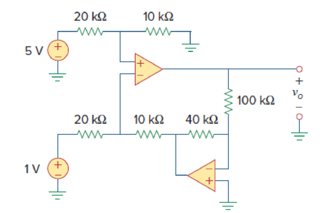
Determine vo in the op amp circuit of Fig. 5.102, using PSpice or MultiSim.
Expert Solution & Answer
Want to see the full answer?
Check out a sample textbook solution
Students have asked these similar questions
Q1: Design a logic circuit for the finite-state machine described by the assigned
table in Fig. 1:
Using D flip-flops.
a.
b.
Using T flip-flops.
Present
Next State
Output
State
x=0
x=0
YE
Y₁Y
Y₁Y
Z
00
00
01
0
0
от
00
0
0
10
00
10
11
00
10
0
Find Va and Vb using mesh analysis
Find Va and Vb using Mesh analysis
Chapter 5 Solutions
Fundamentals of Electric Circuits
Ch. 5.2 - If the same 741 op amp in Example 5.1 is used in...Ch. 5.3 - Repeat Example 5.1 using the ideal op amp model....Ch. 5.4 - Practice Problem 5.3 Figure 5.13 For Practice...Ch. 5.4 - Two kinds of current-to-voltage converters (also...Ch. 5.5 - Calculate vo in the circuit of Fig. 5.20. Answer:...Ch. 5.6 - Practice Problem 5.6 Find vo and io in the op amp...Ch. 5.7 - Design a difference amplifier with gain 7.5....Ch. 5.7 - Obtain io in the instrumentation amplifier circuit...Ch. 5.8 - Practice Problem 5.9 Figure 5.30 For Practice...Ch. 5.8 - If v1 = 5 V and v2 = 5 V, find vo in the op amp...
Ch. 5.9 - Rework Practice Prob. 5.1 using PSpice. If the...Ch. 5.10 - A three-bit DAC is shown in Fig. 5.37. (a)...Ch. 5.10 - Determine the value of the external gain-setting...Ch. 5 - The two input terminals of an op amp are labeled...Ch. 5 - For an ideal op amp, which of the following...Ch. 5 - For the circuit in Fig. 5.40, voltage vo is: (a)6...Ch. 5 - For the circuit in Fig. 5.40, current ix is:...Ch. 5 - If vs = 0 in the circuit of Fig. 5.41, current io...Ch. 5 - If vs = 8 mV in the circuit of Fig. 5.41, the...Ch. 5 - Refer to Fig. 5.41. If vs = 8 mV, voltage va is:...Ch. 5 - The power absorbed by the 4-k resistor in Fig....Ch. 5 - Which of these amplifiers is used in a...Ch. 5 - Difference amplifiers are used in (please check...Ch. 5 - The equivalent model of a certain op amp is shown...Ch. 5 - The open-loop gain of an op amp is 50,000....Ch. 5 - Determine the voltage input to the inverting...Ch. 5 - The output voltage of an op amp is 4 V when the...Ch. 5 - For the op amp circuit of Fig. 5.44, the op amp...Ch. 5 - Using the same parameters for the 741 op amp in...Ch. 5 - 5.7 The op amp in Fig. 5.46 has Ri = 100 k, Ro =...Ch. 5 - Obtain vo for each of the op amp circuits in Fig....Ch. 5 - Determine vo for each of the op amp circuits in...Ch. 5 - Prob. 10PCh. 5 - Using Fig. 5.50, design a problem to help other...Ch. 5 - Calculate the voltage ratio vo/vs for the op amp...Ch. 5 - Find vo and io in the circuit of Fig. 5.52. Figure...Ch. 5 - Determine the output voltage vo in the circuit of...Ch. 5 - (a)Determine the ratio vo/is in the op amp circuit...Ch. 5 - Using Fig. 5.55, design a problem to help students...Ch. 5 - Prob. 17PCh. 5 - For the circuit shown in Figure 5.57, solve for...Ch. 5 - Determine io in the circuit of Fig. 5.58. Figure...Ch. 5 - In the circuit of Fig. 5.59, calculate vo of vs =...Ch. 5 - Calculate vo in the op amp circuit of Fig. 5.60....Ch. 5 - Design an inverting amplifier with a gain of 15.Ch. 5 - For the op amp circuit in Fig. 5.61, find the...Ch. 5 - In the circuit shown in Fig. 5.62, find k in the...Ch. 5 - Calculate vo in the op amp circuit of Fig. 5.63....Ch. 5 - Using Fig. 5.64, design a problem to help other...Ch. 5 - Find vo in the op amp circuit of Fig. 5.65. Figure...Ch. 5 - Prob. 28PCh. 5 - Determine the voltage gain vo/vi of the op amp...Ch. 5 - In the circuit shown in Fig. 5.68, find ix and the...Ch. 5 - For the circuit in Fig. 5.69, find ix. Figure 5.69...Ch. 5 - Calculate ix and vo in the circuit of Fig. 5.70....Ch. 5 - Refer to the op amp circuit in Fig. 5.71....Ch. 5 - Given the op amp circuit shown in Fig. 5.72,...Ch. 5 - Design a noninverting amplifier with a gain of...Ch. 5 - For the circuit shown in Fig. 5.73, find the...Ch. 5 - Determine the output of the summing amplifier in...Ch. 5 - Using Fig. 5.75, design a problem to help other...Ch. 5 - For the op amp circuit in Fig. 5.76, determine the...Ch. 5 - Referring to the circuit shown in Fig. 5.77,...Ch. 5 - An averaging amplifier is a summer that provides...Ch. 5 - The feedback resistor of a three-input averaging...Ch. 5 - The feedback resistor of a five-input averaging...Ch. 5 - Show that the output voltage vo of the circuit in...Ch. 5 - Design an op amp circuit to perform the following...Ch. 5 - Using only two op amps, design a circuit to solve...Ch. 5 - The circuit in Fig. 5.79 is for a difference...Ch. 5 - The circuit in Fig. 5.80 is a differential...Ch. 5 - Design a difference amplifier to have a gain of 4...Ch. 5 - Design a circuit to amplify the difference between...Ch. 5 - Using two op amps, design a subtractor.Ch. 5 - Design an op amp circuit such that vo = 4v1 + 6v2 ...Ch. 5 - The ordinary difference amplifier for fixed-gain...Ch. 5 - Determine the voltage transfer ratio vovs in the...Ch. 5 - In a certain electronic device, a three-stage...Ch. 5 - Using Fig. 5.83, design a problem to help other...Ch. 5 - Find vo in the op amp circuit of Fig. 5.84.Ch. 5 - Calculate io in the op amp circuit of Fig. 5.85....Ch. 5 - In the op amp circuit of Fig. 5.86, determine the...Ch. 5 - Calculate vo/vi in the op amp circuit of Fig....Ch. 5 - Determine vo in the circuit of Fig. 5.88. Figure...Ch. 5 - Obtain the closed-loop voltage gain vo/vi of the...Ch. 5 - Determine the gain vovi of the circuit in Fig....Ch. 5 - For the op amp circuit shown in Fig. 5.91, find...Ch. 5 - Find vo in the op amp circuit of Fig. 5.92.Ch. 5 - For the circuit in Fig. 5.93, find vo.Ch. 5 - Obtain the output vo in the circuit of Fig. 5.94....Ch. 5 - Find vo in the circuit of Fig. 5.95, assuming that...Ch. 5 - Find vo in the circuit of Fig. 5.95, assuming that...Ch. 5 - Determine vo in the op amp circuit of Fig. 5.96.Ch. 5 - Determine vo in the op amp circuit of Fig. 5.97.Ch. 5 - Find the load voltage vL in the circuit of Fig....Ch. 5 - Determine the load voltage vL in the circuit of...Ch. 5 - Find io in the op amp circuit of Fig. 5.100....Ch. 5 - Rework Example 5.11 using the nonideal op amp...Ch. 5 - Solve Prob. 5.19 using PSpice or MultiSim and op...Ch. 5 - Solve Prob. 5.48 using PSpice or MultiSim and op...Ch. 5 - Use PSpice or MultiSim to obtain vo in the circuit...Ch. 5 - Determine vo in the op amp circuit of Fig. 5.102,...Ch. 5 - Use PSpice or MultiSim to solve Prob. 5.70....Ch. 5 - Use PSpice or MultiSim to verify the results in...Ch. 5 - Prob. 82PCh. 5 - Design a six-bit digital-to-analog converter. (a)...Ch. 5 - A four-bit R-2R ladder DAC is presented in Fig....Ch. 5 - In the op amp circuit of Fig. 5.104, find the...Ch. 5 - Design a voltage controlled ideal current source...Ch. 5 - Figure 5.105 displays a two-op-amp instrumentation...Ch. 5 - Figure 5.106 shows an instrumentation amplifier...Ch. 5 - Design a circuit that provides a relationship...Ch. 5 - The op amp circuit in Fig. 5.107 is a current...Ch. 5 - A noninverting current amplifier is portrayed in...Ch. 5 - Refer to the bridge amplifier shown in Fig. 5.109....Ch. 5 - A voltage-to-current converter is shown in Fig....
Knowledge Booster


Learn more about
Need a deep-dive on the concept behind this application? Look no further. Learn more about this topic, electrical-engineering and related others by exploring similar questions and additional content below.Similar questions
- Find Va and Vb using nodal analysisarrow_forward2. Using the approximate method, hand sketch the Bode plot for the following transfer functions. a) H(s) = 10 b) H(s) (s+1) c) H(s): = 1 = +1 100 1000 (s+1) 10(s+1) d) H(s) = (s+100) (180+1)arrow_forwardQ4: Write VHDL code to implement the finite-state machine described by the state Diagram in Fig. 1. Fig. 1arrow_forward
- 1. Consider the following feedback system. Bode plot of G(s) is shown below. Phase (deg) Magnitude (dB) -50 -100 -150 -200 0 -90 -180 -270 101 System: sys Frequency (rad/s): 0.117 Magnitude (dB): -74 10° K G(s) Bode Diagram System: sys Frequency (rad/s): 36.8 Magnitude (dB): -99.7 System: sys Frequency (rad/s): 20 Magnitude (dB): -89.9 System: sys Frequency (rad/s): 20 Phase (deg): -143 System: sys Frequency (rad/s): 36.8 Phase (deg): -180 101 Frequency (rad/s) a) Determine the range of K for which the closed-loop system is stable. 102 10³ b) If we want the gain margin to be exactly 50 dB, what is value for K we should choose? c) If we want the phase margin to be exactly 37°, what is value of K we should choose? What will be the corresponding rise time (T) for step-input? d) If we want steady-state error of step input to be 0.6, what is value of K we should choose?arrow_forward: Write VHDL code to implement the finite-state machine/described by the state Diagram in Fig. 4. X=1 X=0 solo X=1 X=0 $1/1 X=0 X=1 X=1 52/2 $3/3 X=1 Fig. 4 X=1 X=1 56/6 $5/5 X=1 54/4 X=0 X-O X=O 5=0 57/7arrow_forwardQuestions: Q1: Verify that the average power generated equals the average power absorbed using the simulated values in Table 7-2. Q2: Verify that the reactive power generated equals the reactive power absorbed using the simulated values in Table 7-2. Q3: Why it is important to correct the power factor of a load? Q4: Find the ideal value of the capacitor theoretically that will result in unity power factor. Vs pp (V) VRIPP (V) VRLC PP (V) AT (μs) T (us) 8° pf Simulated 14 8.523 7.84 84.850 1000 29.88 0.866 Measured 14 8.523 7.854 82.94 1000 29.85 0.86733 Table 7-2 Power Calculations Pvs (mW) Qvs (mVAR) PRI (MW) Pay (mW) Qt (mVAR) Qc (mYAR) Simulated -12.93 -7.428 9.081 3.855 12.27 -4.84 Calculated -12.936 -7.434 9.083 3.856 12.32 -4.85 Part II: Power Factor Correction Table 7-3 Power Factor Correction AT (us) 0° pf Simulated 0 0 1 Measured 0 0 1arrow_forward
- Questions: Q1: Verify that the average power generated equals the average power absorbed using the simulated values in Table 7-2. Q2: Verify that the reactive power generated equals the reactive power absorbed using the simulated values in Table 7-2. Q3: Why it is important to correct the power factor of a load? Q4: Find the ideal value of the capacitor theoretically that will result in unity power factor. Vs pp (V) VRIPP (V) VRLC PP (V) AT (μs) T (us) 8° pf Simulated 14 8.523 7.84 84.850 1000 29.88 0.866 Measured 14 8.523 7.854 82.94 1000 29.85 0.86733 Table 7-2 Power Calculations Pvs (mW) Qvs (mVAR) PRI (MW) Pay (mW) Qt (mVAR) Qc (mYAR) Simulated -12.93 -7.428 9.081 3.855 12.27 -4.84 Calculated -12.936 -7.434 9.083 3.856 12.32 -4.85 Part II: Power Factor Correction Table 7-3 Power Factor Correction AT (us) 0° pf Simulated 0 0 1 Measured 0 0 1arrow_forwardelectric plants. Prepare the load schedulearrow_forwardelectric plants Draw the column diagram. Calculate the voltage drop. by hand writingarrow_forward
- electric plants. Draw the lighting, socket, telephone, TV, and doorbell installations on the given single-story project with an architectural plan by hand writingarrow_forwardA circularly polarized wave, traveling in the +z-direction, is received by an elliptically polarized antenna whose reception characteristics near the main lobe are given approx- imately by E„ = [2â, + jâ‚]ƒ(r. 8, 4) Find the polarization loss factor PLF (dimensionless and in dB) when the incident wave is (a) right-hand (CW) An elliptically polarized wave traveling in the negative z-direction is received by a circularly polarized antenna. The vector describing the polarization of the incident wave is given by Ei= 2ax + jay.Find the polarization loss factor PLF (dimensionless and in dB) when the wave that would be transmitted by the antenna is (a) right-hand CParrow_forwardjX(1)=j0.2p.u. jXa(2)=j0.15p.u. jxa(0)=0.15 p.u. V₁=1/0°p.u. V₂=1/0° p.u. 1 jXr(1) = j0.15 p.11. jXT(2) = j0.15 p.u. jXr(0) = j0.15 p.u. V3=1/0° p.u. А V4=1/0° p.u. 2 jX1(1)=j0.12 p.u. 3 jX2(1)=j0.15 p.u. 4 jX1(2)=0.12 p.11. JX1(0)=0.3 p.u. jX/2(2)=j0.15 p.11. X2(0)=/0.25 p.1. Figure 1. Circuit for Q3 b).arrow_forward
arrow_back_ios
SEE MORE QUESTIONS
arrow_forward_ios
Recommended textbooks for you
 Introductory Circuit Analysis (13th Edition)Electrical EngineeringISBN:9780133923605Author:Robert L. BoylestadPublisher:PEARSON
 Delmar's Standard Textbook Of ElectricityElectrical EngineeringISBN:9781337900348Author:Stephen L. HermanPublisher:Cengage Learning
 Programmable Logic ControllersElectrical EngineeringISBN:9780073373843Author:Frank D. PetruzellaPublisher:McGraw-Hill Education
 Fundamentals of Electric CircuitsElectrical EngineeringISBN:9780078028229Author:Charles K Alexander, Matthew SadikuPublisher:McGraw-Hill Education
 Electric Circuits. (11th Edition)Electrical EngineeringISBN:9780134746968Author:James W. Nilsson, Susan RiedelPublisher:PEARSON
 Engineering ElectromagneticsElectrical EngineeringISBN:9780078028151Author:Hayt, William H. (william Hart), Jr, BUCK, John A.Publisher:Mcgraw-hill Education,
Introductory Circuit Analysis (13th Edition)
Electrical Engineering
ISBN:9780133923605
Author:Robert L. Boylestad
Publisher:PEARSON
Delmar's Standard Textbook Of Electricity
Electrical Engineering
ISBN:9781337900348
Author:Stephen L. Herman
Publisher:Cengage Learning
Programmable Logic Controllers
Electrical Engineering
ISBN:9780073373843
Author:Frank D. Petruzella
Publisher:McGraw-Hill Education
Fundamentals of Electric Circuits
Electrical Engineering
ISBN:9780078028229
Author:Charles K Alexander, Matthew Sadiku
Publisher:McGraw-Hill Education
Electric Circuits. (11th Edition)
Electrical Engineering
ISBN:9780134746968
Author:James W. Nilsson, Susan Riedel
Publisher:PEARSON
Engineering Electromagnetics
Electrical Engineering
ISBN:9780078028151
Author:Hayt, William H. (william Hart), Jr, BUCK, John A.
Publisher:Mcgraw-hill Education,
Z Parameters - Impedance Parameters; Author: Electrical Engineering Authority;https://www.youtube.com/watch?v=qoD4AoNmySA;License: Standard Youtube License