Concept explainers
Videos
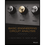
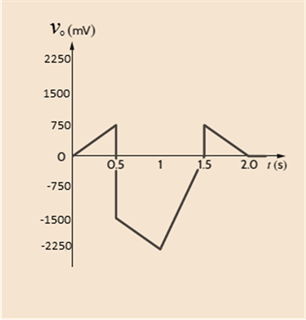
An amplifier has a gain of 15 and the input waveform shown in Fig. P4.1. Draw the output waveform.
To draw:
The output waveform using input waveform and gain of the amplifier.
Explanation of Solution
Given:
Amplifier has a gain of 15 and input waveform shown below.
Calculation:
For an amplifier, output voltage is product of gain and its input voltage.
In the given figure, calculate the output voltage by the above formulae at different time to form a graph.
At
At
At
At
At
The output waveform for the given input is shown below.
Want to see more full solutions like this?
Chapter 4 Solutions
Basic Engineering Circuit Analysis


- I need help with this problem and an step by step explanation of the solution from the image described below. (Introduction to Signals and Systems)arrow_forwardi need help insolving the following question pleasearrow_forwardI need help with this problem and an step by step explanation of the solution from the image described below. (Introduction to Signals and Systems)arrow_forward
- i need help insolving the following question pleasearrow_forwardNote that all capacitors are large so that their impedance is negligible at signal frequencies of interest. npn equations active Ic Ise VBE/VT = IB = (Is/B)eVB VBE/VT IE = (Is/α)еVB VBE/VT Ic=ẞIB_IС = αIE B α α = B = B+1 1-α Ic α Im Υπ re To= VT 9m Im 550 VAarrow_forwardi need help insolving the following question pleasearrow_forward
- I need help with this problem and an step by step explanation of the solution from the image described below. (Introduction to Signals and Systems)arrow_forward10.49 Using source transformation, find i in the circuit of Fig. 10.94. 5 Ω www 3Ω 5 mH 8 sin(200t+30°) A 1 mFarrow_forwardThis exam is closed book, but you may use one 8.5x11" sheet of notes (both sides), handwritten by you Wote all answers kot on this test paper! Use the personal key number N (written above) on the parameters se fix to Show your work and explain your reasoning Partial credit will be given for partial solutions. When giving a numerical answer, specify units ill any apply. No credit will be given for solving problems from previous 1. For the AM signal with periodic message m() shown in Fig. 1 and modulation index = 0.03A a) find the carrier amplitude and carrier power; b) find the sideband power and compute the power efficiency & N = 15 4+N AA -(4+N) Fig. 1 r(s)→arrow_forward
 Introductory Circuit Analysis (13th Edition)Electrical EngineeringISBN:9780133923605Author:Robert L. BoylestadPublisher:PEARSON
 Delmar's Standard Textbook Of ElectricityElectrical EngineeringISBN:9781337900348Author:Stephen L. HermanPublisher:Cengage Learning
 Programmable Logic ControllersElectrical EngineeringISBN:9780073373843Author:Frank D. PetruzellaPublisher:McGraw-Hill Education
 Fundamentals of Electric CircuitsElectrical EngineeringISBN:9780078028229Author:Charles K Alexander, Matthew SadikuPublisher:McGraw-Hill Education
 Electric Circuits. (11th Edition)Electrical EngineeringISBN:9780134746968Author:James W. Nilsson, Susan RiedelPublisher:PEARSON
 Engineering ElectromagneticsElectrical EngineeringISBN:9780078028151Author:Hayt, William H. (william Hart), Jr, BUCK, John A.Publisher:Mcgraw-hill Education,