
MICROELECT. CIRCUIT ANALYSIS&DESIGN (LL)
4th Edition
ISBN: 9781266368622
Author: NEAMEN
Publisher: MCG
expand_more
expand_more
format_list_bulleted
Videos
Textbook Question
Chapter 3, Problem 3.41P
Design the circuit in Figure P3.41 so that
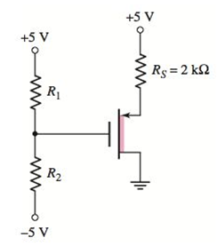
Figure P3.41
Expert Solution & Answer
Want to see the full answer?
Check out a sample textbook solution
Students have asked these similar questions
A conductor 300 mm long carries a current of 13A and is at right-angles to a magnetic fieldbetween two circular pole faces, each of diameter 80 mm. If the total flux between the polefaces is 0.75 mWb, calculate the force exerted on the conductor. [ANS = 0.582 N]
a) find Rthb) Find Vth in the circuit
c)Draw the Thevenin Equivalent of the circuit to tge left of the a and b terminals
An electric car runs on batteries, but needs to make constant stops to re-charge. If a trailer is attached to the car that carries a generator, and the generator is turned by a belt attached to the wheels of the trailer, will the car be able to drive forever without stopping?
Chapter 3 Solutions
MICROELECT. CIRCUIT ANALYSIS&DESIGN (LL)
Ch. 3 - An NMOS transistor with VTN=1V has a drain current...Ch. 3 - An PMOS device with VTP=1.2V has a drain current...Ch. 3 - (a) An nchannel enhancementmode MOSFET has a...Ch. 3 - The NMOS devices described in Exercise TYU 3.1...Ch. 3 - (a) A pchannel enhancementmode MOSFET has a...Ch. 3 - The PMOS devices described in Exercise TYU 3.3...Ch. 3 - The parameters of an NMOS enhancementmode device...Ch. 3 - An NMOS transistor has parameters VTNO=0.4V ,...Ch. 3 - Prob. 3.3EPCh. 3 - The transistor in Figure 3.26(a) has parameters...
Ch. 3 - For the transistor in the circuit in Figure 3.28,...Ch. 3 - Consider the circuit shown in Figure 3.30. The...Ch. 3 - Consider the circuit in Figure 3.30. Using the...Ch. 3 - (a) Consider the circuit shown in Figure 3.33. The...Ch. 3 - Consider the NMOS inverter shown in Figure 3.36...Ch. 3 - Consider the circuit shown in Figure 3.39 with...Ch. 3 - Consider the circuit in Figure 3.41. Assume the...Ch. 3 - Prob. 3.7TYUCh. 3 - Consider the circuit in Figure 3.43. The...Ch. 3 - For the circuit shown in Figure 3.36, use the...Ch. 3 - Consider the circuit shown in Figure 3.44. The...Ch. 3 - For the circuit shown in Figure 3.39, use the...Ch. 3 - For the MOS inverter circuit shown in Figure 3.45,...Ch. 3 - For the circuit in Figure 3.46, assume the circuit...Ch. 3 - The circuit shown in Figure 3.45 is biased at...Ch. 3 - The transistor in the circuit shown in Figure 3.48...Ch. 3 - In the circuit in Figure 3.46, let RD=25k and...Ch. 3 - For the circuit shown in Figure 3.49(a), assume...Ch. 3 - Prob. 3.15EPCh. 3 - Consider the constantcurrent source shown in...Ch. 3 - Consider the circuit in Figure 3.49(b). Assume...Ch. 3 - Consider the circuit shown in Figure 3.50. Assume...Ch. 3 - The transistor parameters for the circuit shown in...Ch. 3 - The transistor parameters for the circuit shown in...Ch. 3 - The parameters of an nchannel JFET are IDSS=12mA ,...Ch. 3 - The transistor in the circuit in Figure 3.62 has...Ch. 3 - For the pchannel transistor in the circuit in...Ch. 3 - Consider the circuit shown in Figure 3.66 with...Ch. 3 - The nchannel enhancementmode MESFET in the circuit...Ch. 3 - For the inverter circuit shown in Figure 3.68, the...Ch. 3 - Describe the basic structure and operation of a...Ch. 3 - Sketch the general currentvoltage characteristics...Ch. 3 - Describe what is meant by threshold voltage,...Ch. 3 - Describe the channel length modulation effect and...Ch. 3 - Describe a simple commonsource MOSFET circuit with...Ch. 3 - Prob. 6RQCh. 3 - In the dc analysis of some MOSFET circuits,...Ch. 3 - Prob. 8RQCh. 3 - Describe the currentvoltage relation of an...Ch. 3 - Describe the currentvoltage relation of an...Ch. 3 - Prob. 11RQCh. 3 - Describe how a MOSFET can be used to amplify a...Ch. 3 - Describe the basic operation of a junction FET.Ch. 3 - Prob. 14RQCh. 3 - (a) Calculate the drain current in an NMOS...Ch. 3 - The current in an NMOS transistor is 0.5 mA when...Ch. 3 - The transistor characteristics iD versus VDS for...Ch. 3 - For an nchannel depletionmode MOSFET, the...Ch. 3 - Verify the results of Example 3.4 with a PSpice...Ch. 3 - The threshold voltage of each transistor in Figure...Ch. 3 - The threshold voltage of each transistor in Figure...Ch. 3 - Consider an nchannel depletionmode MOSFET with...Ch. 3 - Determine the value of the process conduction...Ch. 3 - An nchannel enhancementmode MOSFET has parameters...Ch. 3 - Consider the NMOS circuit shown in Figure 3.36....Ch. 3 - An NMOS device has parameters VTN=0.8V , L=0.8m ,...Ch. 3 - Consider the NMOS circuit shown in Figure 3.39....Ch. 3 - A particular NMOS device has parameters VTN=0.6V ,...Ch. 3 - MOS transistors with very short channels do not...Ch. 3 - For a pchannel enhancementmode MOSFET, kp=50A/V2 ....Ch. 3 - For a pchannel enhancementmode MOSFET, the...Ch. 3 - The transistor characteristics iD versus SD for a...Ch. 3 - A pchannel depletionmode MOSFET has parameters...Ch. 3 - Calculate the drain current in a PMOS transistor...Ch. 3 - sDetermine the value of the process conduction...Ch. 3 - Enhancementmode NMOS and PMOS devices both have...Ch. 3 - For an NMOS enhancementmode transistor, the...Ch. 3 - The parameters of an nchannel enhancementmode...Ch. 3 - An enhancementmode NMOS transistor has parameters...Ch. 3 - An NMOS transistor has parameters VTO=0.75V ,...Ch. 3 - (a) A silicon dioxide gate insulator of an MOS...Ch. 3 - In a power MOS transistor, the maximum applied...Ch. 3 - In the circuit in Figure P3.26, the transistor...Ch. 3 - The transistor in the circuit in Figure P3.27 has...Ch. 3 - Prob. D3.28PCh. 3 - The transistor in the circuit in Figure P3.29 has...Ch. 3 - Consider the circuit in Figure P3.30. The...Ch. 3 - For the circuit in Figure P3.31, the transistor...Ch. 3 - Design a MOSFET circuit in the configuration shown...Ch. 3 - Consider the circuit shown in Figure P3.33. The...Ch. 3 - The transistor parameters for the transistor in...Ch. 3 - For the transistor in the circuit in Figure P3.35,...Ch. 3 - Design a MOSFET circuit with the configuration...Ch. 3 - The parameters of the transistors in Figures P3.37...Ch. 3 - For the circuit in Figure P3.38, the transistor...Ch. 3 - Prob. 3.39PCh. 3 - Prob. 3.40PCh. 3 - Design the circuit in Figure P3.41 so that...Ch. 3 - Prob. 3.42PCh. 3 - Prob. 3.43PCh. 3 - Prob. 3.44PCh. 3 - Prob. 3.45PCh. 3 - Prob. 3.46PCh. 3 - Prob. 3.47PCh. 3 - The transistors in the circuit in Figure 3.36 in...Ch. 3 - For the circuit in Figure 3.39 in the text, the...Ch. 3 - Prob. 3.50PCh. 3 - The transistor in the circuit in Figure P3.51 is...Ch. 3 - Prob. 3.52PCh. 3 - For the twoinput NMOS NOR logic gate in Figure...Ch. 3 - All transistors in the currentsource circuit shown...Ch. 3 - All transistors in the currentsource circuit shown...Ch. 3 - Consider the circuit shown in Figure 3.50 in the...Ch. 3 - The gate and source of an nchannel depletionmode...Ch. 3 - For an nchannel JFET, the parameters are IDSS=6mA...Ch. 3 - A pchannel JFET biased in the saturation region...Ch. 3 - Prob. 3.60PCh. 3 - Prob. 3.61PCh. 3 - The threshold voltage of a GaAs MESFET is...Ch. 3 - Prob. 3.63PCh. 3 - Prob. 3.64PCh. 3 - Prob. 3.65PCh. 3 - For the circuit in Figure P3.66, the transistor...Ch. 3 - Prob. 3.67PCh. 3 - Prob. 3.68PCh. 3 - For the circuit in Figure P3.69, the transistor...Ch. 3 - Prob. 3.70PCh. 3 - Prob. 3.71PCh. 3 - Prob. 3.72PCh. 3 - Using a computer simulation, verify the results of...Ch. 3 - Consider the PMOS circuit shown in Figure 3.30....Ch. 3 - Consider the circuit in Figure 3.39 with a...Ch. 3 - Prob. D3.79DPCh. 3 - Consider the multitransistor circuit in Figure...
Knowledge Booster


Learn more about
Need a deep-dive on the concept behind this application? Look no further. Learn more about this topic, electrical-engineering and related others by exploring similar questions and additional content below.Similar questions
- A singl core cable of voltage 30 kv. The diameter of Conductor is 3 cm. The diameter of cable is 25 cm. This cable has Two layer of insulator having arelative permittivity 5-3 respectively of The ratio of maximum electric stress of maximum electric stress 8 First layer to the of second layer is 10 Find & 1- The thickness of each layers. 3- The voltage of each layers. §. Layers The saving in radius of cable if another ungrading cable has the Same maximum electric stress, Total village, Conductor diameter of grading cable.arrow_forward66 KV sing care Cable has a drameter of conductor of 3 cm. The radius of cable is 10 cm. This Cable house Two relative permmitivity of insulation 6 and 4 respectively. If The ratio of maximum electric stress of first layer to the maximum eledric streep & second layer is s 1- find the village & each layers. 2- Min- electric stress J Cable 3- Compare the voltage of ungrading Cable has the same distance and relectric stresses.arrow_forwardPrelab Information 1. Laboratory Preliminary Discussion First-order Low-pass RC Filter Analysis The first-order low-pass RC filter shown in figure 1 below represents all voltages and currents in the time domain. It is of course possible to solve for all circuit voltages using time domain differential equation techniques, but it is more efficient to convert the circuit to its s-domain equivalent as shown in figure 2 and apply Laplace transform techniques. vs(t) i₁(t) + R₁ ww V₁(t) 12(t) Lic(t) Vout(t) = V2(t) R₂ Vc(t) C Vc(t) VR2(t) = V2(t) + Vs(s) Figure 1: A first-order low-pass RC filter represented in the time domain. I₁(s) R1 W + V₁(s) V₂(s) 12(s) Ic(s) + Vout(S) == Vc(s) Vc(s) Zc(s) = = VR2(S) V2(s) Figure 2: A first-order low-pass RC filter represented in the s-domain.arrow_forward
- Solve it in a different way than the previous solution that I searched forarrow_forwardA lossless uncharged transmission line of length L = 0.45 cm has a characteristic impedance of 60 ohms. It is driven by an ideal voltage generator producing a pulse of amplitude 10V and width 2 nS. If the transmission line is connected to a load of 200 ohms, sketch the voltage at the load as a function of time for the interval 0 < t < 20 nS. You may assume that the propagation velocity of the transmission is c/2. Answered now answer number 2. Repeat Q.1 but now assume the width of the pulse produced by the generator is 4 nS. Sketch the voltage at the load as a function of time for 0 < t < 20 nS.arrow_forwardSolve this experiment with an accurate solution, please. Thank you.arrow_forward
- A lossless uncharged transmission line of characteristic impedance Zo = 600 and length T = 1us is connected to a 180 load. If this transmission line is connected at t = 0 to a 90 V dc source with an internal resistance of 900, from a bounce diagram of this system sketch (a) the voltage at z=0, z=L, and z = L/2 for up to 7.25μs and (b) calculate the load voltage after an infinite amount of time.arrow_forwardA lossless uncharged transmission line of length L = 0.45 cm has a characteristic impedance of 60 ohms. It is driven by an ideal voltage generator producing a pulse of amplitude 10V and width 2 nS. If the transmission line is connected to a load of 200 ohms, sketch the voltage at the load as a function of time for the interval 0 < t < 20 nS. You may assume that the propagation velocity of the transmission is c/2.arrow_forwardThe VSWR (Voltage Standing Wave Ratio) is measured to be 2 on a transmission line. Find two values of the reflection coefficient with one corresponding to Z > Zo and the other to Zarrow_forwardarrow_back_iosSEE MORE QUESTIONSarrow_forward_ios
Recommended textbooks for you
 Introductory Circuit Analysis (13th Edition)Electrical EngineeringISBN:9780133923605Author:Robert L. BoylestadPublisher:PEARSON
 Delmar's Standard Textbook Of ElectricityElectrical EngineeringISBN:9781337900348Author:Stephen L. HermanPublisher:Cengage Learning
 Programmable Logic ControllersElectrical EngineeringISBN:9780073373843Author:Frank D. PetruzellaPublisher:McGraw-Hill Education
 Fundamentals of Electric CircuitsElectrical EngineeringISBN:9780078028229Author:Charles K Alexander, Matthew SadikuPublisher:McGraw-Hill Education
 Electric Circuits. (11th Edition)Electrical EngineeringISBN:9780134746968Author:James W. Nilsson, Susan RiedelPublisher:PEARSON
 Engineering ElectromagneticsElectrical EngineeringISBN:9780078028151Author:Hayt, William H. (william Hart), Jr, BUCK, John A.Publisher:Mcgraw-hill Education,
Introductory Circuit Analysis (13th Edition)
Electrical Engineering
ISBN:9780133923605
Author:Robert L. Boylestad
Publisher:PEARSON
Delmar's Standard Textbook Of Electricity
Electrical Engineering
ISBN:9781337900348
Author:Stephen L. Herman
Publisher:Cengage Learning
Programmable Logic Controllers
Electrical Engineering
ISBN:9780073373843
Author:Frank D. Petruzella
Publisher:McGraw-Hill Education
Fundamentals of Electric Circuits
Electrical Engineering
ISBN:9780078028229
Author:Charles K Alexander, Matthew Sadiku
Publisher:McGraw-Hill Education
Electric Circuits. (11th Edition)
Electrical Engineering
ISBN:9780134746968
Author:James W. Nilsson, Susan Riedel
Publisher:PEARSON
Engineering Electromagnetics
Electrical Engineering
ISBN:9780078028151
Author:Hayt, William H. (william Hart), Jr, BUCK, John A.
Publisher:Mcgraw-hill Education,
Diode Logic Gates - OR, NOR, AND, & NAND; Author: The Organic Chemistry Tutor;https://www.youtube.com/watch?v=9lqwSaIDm2g;License: Standard Youtube License