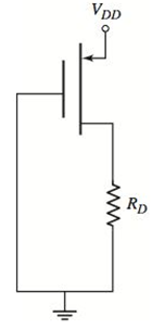
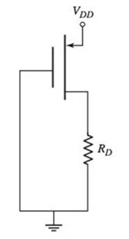
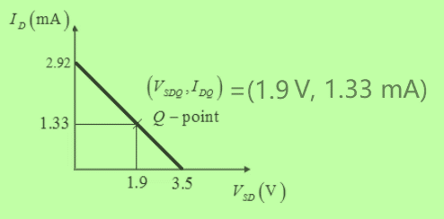
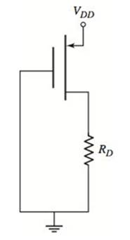
Problem 3.1EP: An NMOS transistor with VTN=1V has a drain current iD=0.8mA when GS=3V and DS=4.5V Calculate the... Problem 3.2EP: An PMOS device with VTP=1.2V has a drain current iD=0.5mA when GS=3V and SD=5V . Calculate the drain... Problem 3.1TYU: (a) An nchannel enhancementmode MOSFET has a threshold voltage of VTN=1.2V and an applied... Problem 3.2TYU: The NMOS devices described in Exercise TYU 3.1 have parameters W=20m , L=0.8m , to tox=200 ,... Problem 3.3TYU: (a) A pchannel enhancementmode MOSFET has a threshold voltage of VTP=1.2V and an applied... Problem 3.4TYU: The PMOS devices described in Exercise TYU 3.3 have parameters W=10m , L=0.8m , tox=200 ,... Problem 3.5TYU: The parameters of an NMOS enhancementmode device are VTN=0.25V and Kn=10A/V2 . The device is biased... Problem 3.6TYU: An NMOS transistor has parameters VTNO=0.4V , =0.15V1/2 , and f=0.345V . Calculate the threshold... Problem 3.3EP Problem 3.4EP: The transistor in Figure 3.26(a) has parameters VTP=0.6V and Kp=0.2mA/V2 . The circuit is biased at... Problem 3.5EP: For the transistor in the circuit in Figure 3.28, the nominal parameter values are VTN=0.6V and... Problem 3.6EP: Consider the circuit shown in Figure 3.30. The nominal transistor parameters are VTP=0.30V and... Problem 3.7EP: Consider the circuit in Figure 3.30. Using the nominal transistor parameters described in Exercise... Problem 3.8EP: (a) Consider the circuit shown in Figure 3.33. The transistor parameters are VTP=0.40V and Kp=30A/V2... Problem 3.9EP: Consider the NMOS inverter shown in Figure 3.36 with transistor parameters described in Example 3.9.... Problem 3.10EP: Consider the circuit shown in Figure 3.39 with transistor parameters VTND=1V and VTNL=2V . (a)... Problem 3.11EP: Consider the circuit in Figure 3.41. Assume the same transistor parameters and circuit parameters as... Problem 3.7TYU Problem 3.8TYU: Consider the circuit in Figure 3.43. The transistor parameters are VTN=0.4V and kn=100A/V2 . Design... Problem 3.9TYU: For the circuit shown in Figure 3.36, use the transistor parameters given in Example 3.9. (a)... Problem 3.10TYU: Consider the circuit shown in Figure 3.44. The transistor parameters are VTN=1.2V and kn=80A/V2 .... Problem 3.11TYU: For the circuit shown in Figure 3.39, use the transistor parameters given in Example 3.10. (a)... Problem 3.12EP: For the MOS inverter circuit shown in Figure 3.45, assume the circuit values are VDD=5V and RD=500 .... Problem 3.13EP: For the circuit in Figure 3.46, assume the circuit and transistor parameters are: RD=30k , VTN=1V ,... Problem 3.12TYU: The circuit shown in Figure 3.45 is biased at VDD=10V , and the transistor parameter are VTN=0.7V... Problem 3.13TYU: The transistor in the circuit shown in Figure 3.48 has parameters Kn=4mA/V2 and VTN=0.8V , and is... Problem 3.14TYU: In the circuit in Figure 3.46, let RD=25k and VTN=1V . (a) Determine the value of the conduction... Problem 3.14EP: For the circuit shown in Figure 3.49(a), assume circuit parameters of IREF=120A , V+=3V , and V=3V ;... Problem 3.15EP Problem 3.16EP: Consider the constantcurrent source shown in Figure 3.50. Assume that the threshold voltage of each... Problem 3.15TYU: Consider the circuit in Figure 3.49(b). Assume circuit parameters of IREF2=40A , V+=2.5V , V=2.5V ,... Problem 3.16TYU: Consider the circuit shown in Figure 3.50. Assume all transistor threshold voltages are 0.7 V.... Problem 3.17EP: The transistor parameters for the circuit shown in Figure 3.52 are the same as described in Example... Problem 3.18EP: The transistor parameters for the circuit shown in Figure 3.53 are VTN1=VTN2=0.8V , Kn1=Kn2=0.5mA/V2... Problem 3.19EP: The parameters of an nchannel JFET are IDSS=12mA , VP=4.5V , and =0 . Determine VDS(sat) for... Problem 3.20EP: The transistor in the circuit in Figure 3.62 has parameters IDSS=6mA , VP=4V , and =0 . Design the... Problem 3.21EP: For the pchannel transistor in the circuit in Figure 3.64, the parameters are: IDSS=6mA , VP=4V ,... Problem 3.22EP: Consider the circuit shown in Figure 3.66 with transistor parameters IDSS=8mA , VP=4V , and =0 .... Problem 3.17TYU: The nchannel enhancementmode MESFET in the circuit shown in Figure 3.67 has parameters Kn=50A/V2 and... Problem 3.18TYU: For the inverter circuit shown in Figure 3.68, the nchannel enhancementmode MESFET parameters are... Problem 1RQ: Describe the basic structure and operation of a MOSFET. Define enhancement mode and depletion mode. Problem 2RQ: Sketch the general currentvoltage characteristics for both enhancementmode and depletionmode... Problem 3RQ: Describe what is meant by threshold voltage, widthtolength ratio, and drainto source saturation... Problem 4RQ: Describe the channel length modulation effect and define the parameter . Describe the body effect... Problem 5RQ: Describe a simple commonsource MOSFET circuit with an nchannel enhancementmode device and discuss... Problem 6RQ Problem 7RQ: In the dc analysis of some MOSFET circuits, quadratic equations in gate-to-source voltage are... Problem 8RQ Problem 9RQ: Describe the currentvoltage relation of an nchannel enhancementmode MOSFET with the gate connected... Problem 10RQ: Describe the currentvoltage relation of an nchannel depletionmode MOSFET with the gate connected to... Problem 11RQ Problem 12RQ: Describe how a MOSFET can be used to amplify a timevarying voltage. Problem 13RQ: Describe the basic operation of a junction FET. Problem 14RQ Problem 3.1P: (a) Calculate the drain current in an NMOS transistor with parameters VTN=0.4V , kn=120A/V2 , W=10m... Problem 3.2P: The current in an NMOS transistor is 0.5 mA when VGSVTN=0.6V and 1.0 mA when VGSVTN=1.0V . The... Problem 3.3P: The transistor characteristics iD versus VDS for an NMOS device are shown in Figure P3.3. (a) Is... Problem 3.4P: For an nchannel depletionmode MOSFET, the parameters are VTN=2.5V and Kn=1.1mA/V2 . (a) Determine ID... Problem 3.1CAE: Verify the results of Example 3.4 with a PSpice analysis. As Example 3.4 illustrated, we may not... Problem 3.5P: The threshold voltage of each transistor in Figure P3.5 is VTN=0.4V . Determine the region of... Problem 3.6P: The threshold voltage of each transistor in Figure P3.6 is VTP=0.4V . Determine the region of... Problem 3.7P: Consider an nchannel depletionmode MOSFET with parameters VTN=1.2V and kn=120A/V2 . The drain... Problem 3.8P: Determine the value of the process conduction parameter kn for an NMOS transistor with n=600cm2/Vs... Problem 3.9P: An nchannel enhancementmode MOSFET has parameters VTN=0.4V , W=20m , L=0.8m , tox=200 , and... Problem 3.3CAE: Consider the NMOS circuit shown in Figure 3.36. Plot the voltage transfer characteristics, using a... Problem 3.10P: An NMOS device has parameters VTN=0.8V , L=0.8m , and kn=120A/V2 . When the transistor is biased in... Problem 3.4CAE: Consider the NMOS circuit shown in Figure 3.39. Plot the voltage transfer characteristics using a... Problem 3.11P: A particular NMOS device has parameters VTN=0.6V , L=0.8m , tox=200 , and n=600cm2/Vs . A drain... Problem 3.12P: MOS transistors with very short channels do not exhibit the square law voltage relation in... Problem 3.13P: For a pchannel enhancementmode MOSFET, kp=50A/V2 . The device has drain currents of ID=0.225mA at... Problem 3.14P: For a pchannel enhancementmode MOSFET, the parameters are KP=2mA/V2 and VTP=0.5V . The gate is at... Problem 3.15P: The transistor characteristics iD versus SD for a PMOS device are shown in Figure P3.15. (a) Is this... Problem 3.16P: A pchannel depletionmode MOSFET has parameters VTP=+2V , kp=40A/V2 , and W/L=6 . Determine VSD(sat)... Problem 3.17P: Calculate the drain current in a PMOS transistor with parameters VTP=0.5V , kp=50A/V2 , W=12m ,... Problem 3.18P: sDetermine the value of the process conduction parameter kp for a PMOS transistor with n=250cm2/Vs... Problem 3.19P: Enhancementmode NMOS and PMOS devices both have parameters L=4m and tox=500 A . For the NMOS... Problem 3.20P: For an NMOS enhancementmode transistor, the parameters are: VTN=1.2V , Kn=0.20mA/V2 , and =0.01V1 .... Problem 3.21P: The parameters of an nchannel enhancementmode MOSFET are VTN=0.5V , kn=120A/V2 , and W/L=4 . What is... Problem 3.22P: An enhancementmode NMOS transistor has parameters VTNO=0.8V , =0.8V1/2 , and f=0.35V . At what value... Problem 3.23P: An NMOS transistor has parameters VTO=0.75V , kn=80A/V2 , W/L=15 , f=0.37V , and =0.6V1/2 . (a) The... Problem 3.24P: (a) A silicon dioxide gate insulator of an MOS transistor has a thickness of tox=120 . (i) Calculate... Problem 3.25P: In a power MOS transistor, the maximum applied gate voltage is 24 V. If a safety factor of three is... Problem 3.26P: In the circuit in Figure P3.26, the transistor parameters are VTN=0.8V and Kn=0.5mA/V2 . Calculate... Problem 3.27P: The transistor in the circuit in Figure P3.27 has parameters VTN=0.8V and Kn=0.25mA/V2 . Sketch the... Problem D3.28P Problem 3.29P: The transistor in the circuit in Figure P3.29 has parameters VTP=0.8V and Kp=0.20mA/V2 . Sketch the... Problem 3.30P: Consider the circuit in Figure P3.30. The transistor parameters are VTP=0.8V and Kp=0.5mA/V2 .... Problem 3.31P: For the circuit in Figure P3.31, the transistor parameters are VTP=0.8V and Kp=200A/V2 Determine VS... Problem D3.32P: Design a MOSFET circuit in the configuration shown in Figure P3.26. The transistor parameters are... Problem 3.33P: Consider the circuit shown in Figure P3.33. The transistor parameters are VTN=0.4V and kn=120A/V2 .... Problem 3.34P: The transistor parameters for the transistor in Figure P3.34 are VTN=0.4V , kn=120A/V2 , and W/L=50... Problem 3.35P: For the transistor in the circuit in Figure P3.35, the parameters are VTN=0.4V , kn=120A/V2 , and... Problem D3.36P: Design a MOSFET circuit with the configuration shown in Figure P3.30. The transistor parameters are... Problem 3.37P: The parameters of the transistors in Figures P3.37 (a) and (b) are Kn=0.5mA/V2 , VTN=1.2V , and =0 .... Problem 3.38P: For the circuit in Figure P3.38, the transistor parameters are VTN=0.6V and Kn=200A/V2 . Determine... Problem 3.39P Problem 3.40P Problem 3.41P: Design the circuit in Figure P3.41 so that VSD=2.5V . The current in the bias resistors should be no... Problem 3.42P Problem 3.43P Problem 3.44P Problem 3.45P Problem 3.46P Problem 3.47P Problem 3.48P: The transistors in the circuit in Figure 3.36 in the text have parameters VTN=0.6V , kp=120A/V2 ,... Problem 3.49P: For the circuit in Figure 3.39 in the text, the transistor parameters are: VTND=0.6V , VTNL=1.2V ,... Problem 3.50P Problem 3.51P: The transistor in the circuit in Figure P3.51 is used to turn the LED on and off. The transistor... Problem 3.52P Problem 3.53P: For the twoinput NMOS NOR logic gate in Figure 3.46 in the text, the transistor parameters are... Problem 3.54P: All transistors in the currentsource circuit shown in Figure 3.49(a) in the text have parameters... Problem 3.55P: All transistors in the currentsource circuit shown in Figure 3.49(b) in the text have parameters... Problem 3.56P: Consider the circuit shown in Figure 3.50 in the text. The threshold voltage and process conduction... Problem 3.57P: The gate and source of an nchannel depletionmode WET are connected together. What value of VDS will... Problem 3.58P: For an nchannel JFET, the parameters are IDSS=6mA and VP=3V . Calculate VDS(sat) . If VDSVDS(sat) ,... Problem 3.59P: A pchannel JFET biased in the saturation region with VSD=5V has a drain current of ID=2.8mA at... Problem 3.60P Problem 3.61P Problem 3.62P: The threshold voltage of a GaAs MESFET is VTN=0.24V . The maximum allowable gatetosource voltage is... Problem 3.63P Problem 3.64P Problem 3.65P Problem 3.66P: For the circuit in Figure P3.66, the transistor parameters are IDSS=7mA and VP=3V . Let R1+R2=100k .... Problem 3.67P Problem 3.68P Problem 3.69P: For the circuit in Figure P3.69, the transistor parameters are IDSS=4mA and VP=3V . Design RD such... Problem 3.70P Problem 3.71P Problem 3.72P Problem 3.76CSP: Using a computer simulation, verify the results of Example 3.17 for the multitransistor circuit... Problem D3.77DP: Consider the PMOS circuit shown in Figure 3.30. The circuit is to be redesigned such that IDQ=100A... Problem D3.78DP: Consider the circuit in Figure 3.39 with a depletion load. Assume the circuit is biased at VDD=3.3V... Problem D3.79DP Problem D3.80DP: Consider the multitransistor circuit in Figure 3.52. The bias voltages are changed to V+=3.3V and... format_list_bulleted

 Introductory Circuit Analysis (13th Edition)Electrical EngineeringISBN:9780133923605Author:Robert L. BoylestadPublisher:PEARSON
 Delmar's Standard Textbook Of ElectricityElectrical EngineeringISBN:9781337900348Author:Stephen L. HermanPublisher:Cengage Learning
 Programmable Logic ControllersElectrical EngineeringISBN:9780073373843Author:Frank D. PetruzellaPublisher:McGraw-Hill Education
 Fundamentals of Electric CircuitsElectrical EngineeringISBN:9780078028229Author:Charles K Alexander, Matthew SadikuPublisher:McGraw-Hill Education
 Electric Circuits. (11th Edition)Electrical EngineeringISBN:9780134746968Author:James W. Nilsson, Susan RiedelPublisher:PEARSON
 Engineering ElectromagneticsElectrical EngineeringISBN:9780078028151Author:Hayt, William H. (william Hart), Jr, BUCK, John A.Publisher:Mcgraw-hill Education,


