The change in the output voltages for the kn' parameter change.
b.
Expert Solution
Answer to Problem 3.47P
When kn'=120×1.05=126μA/V2
V1=2.5 V , V2=6 V
When kn'=120×0.95=114μA/V2
V1=2.5 V , V2=6 V
Explanation of Solution
Given Information:
The given values are:
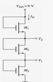
VTN=0.6 V, kn'=120μA/V2,IDQ=0.8 mA, V1=2.5 V, V2=6 V
The given circuit is shown below.
Parameter kn' changes by +5% and −5%
Calculation:
When there is a change in kn' for all transistors with the same percentage, then it will change current through each transistor which is equal in all transistors. According to the below equation, there is no change in VGSQ . So, there is no effect on output voltages V1 and V2 .
IDQ=kn'2(WL)(VGSQ−VTN)2
From part (a), (WL)1=2.315 , (WL)2=1.585 , (WL)3=3.693
2.315(9.3156−2.526V1−0.6)2=3.693(V1−0.6)22.315(9.3156−2.526V1−0.6)2=3.693(V1−0.6)2(9.3156−2.526V1−0.6)=1.263(V1−0.6)V1=9.47343.789 V
V1=2.5 V
From equation (1),
V2=2.526×2.5−0.3156
V2=6 V
So,
When kn'=kn1'=kn2'=kn3'120×1.05=126μA/V2
V1=2.5 V , V2=6 V
When kn'=kn1'=kn2'=kn3'=120×0.95=114μA/V2
V1=2.5 V , V2=6 V
c.
To determine
The output voltages for a specified change in each transistor.
c.
Expert Solution
Answer to Problem 3.47P
V1=2.468 V , V2=5.919 V
Explanation of Solution
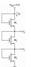
Given Information:
The given values are:
VTN=0.6 V, kn'=120μA/V2,IDQ=0.8 mA, V1=2.5 V, V2=6 V.
The given circuit is shown below.
Also, kn' parameter of M1 decreases by 5% while kn' parameter of M2 and M3 increases by 5%.
Calculation:
When there is a change in kn' for all transistors with the different percentages for transistors, the current through transistors must be equal so that according to the below equation, there may be a change in VGSQ for each transistor. So that output voltages V1 and V2 will change.
IDQ=kn'2(WL)(VGSQ−VTN)2
For M1 :
kn1'=120×0.95=114μA/V2
Now for M2 and M3 :
kn2'=kn3'=120×1.05=126μA/V2
From part(a), (WL)1=2.315 , (WL)2=1.585 , (WL)3=3.693
1142×2.315(9.3156−2.526V1−0.6)2=1262×3.693(V1−0.6)21142×2.315(9.3156−2.526V1−0.6)2=1262×3.693(V1−0.6)2(9.3156−2.526V1−0.6)=1.32784(V1−0.6)V1=9.5123043.85384 V
V1=2.468 V
From equation (1),
V2=2.526×2.468−0.3156
V2=5.919 V
Want to see more full solutions like this?
Subscribe now to access step-by-step solutions to millions of textbook problems written by subject matter experts!
Q3.
a)
The frequency response method enables the study of the steady-state
response of a system G(s). What type of inputs are used for frequency
response? If the system is linear and stable, how does the output differ
from the input? Compare the main characteristics of two types frequency
response plots.
b) Consider the control system shown in Figure Q3.
Controller
E(s)
R(s)
Desired
output
C(s)
Plant
G(s)
Y(s)
Actual
output
3(s + 3)
C(s) = k
G(s) =
= s(s - 1)(s + 10)
Figure Q3. Closed-loop system.
(i) Considering definitions in the study of bounded-input bounded-output
stability, is G(s) stable? Classify the poles and zeros of G(s).
(ii) G(s) defined in Figure Q3 is a system completely characterised by
its transfer function. Explain why this is the case.
(iii) Obtain the closed-loop transfer function P(s) = Y(s)/R(s) of the
system.
(iv) Based on your result for the previous question [Question 3b)-(iii)], use
the Routh-Hurwitz stability criterion to determine suitable values of
gain K…
Please, I want the solution in two ways:
Method 1 (without the Smith chart):
Method 2 (using the Smith chart):
A short circuit stub of length 0.04λ is used to match a 50 Ω lossless line to a load ZL = RL + j30 Ω. Use Smith chart to find:(a) The distance between the stub and the load.(b) The value of RL .
THE FIRST PAGE OF THIS QUESTION SECTION BELOW IS THE FIRST IMAGE UPLOADED, WHICH SHOWS A digital synchronous sequential circuit and then comes the questions below:1B) Suppose the flip-flops are 74F74 devices and the AND gates are 74F08 devices. Let maxtpd,D=9ns, maxtsu,D=3ns, and maxtpd,AND=6ns. What is the maximum clock frequency at which the circuit can operate reliably?
2) Compare serial transmission and parallel transmission and discuss their advantages and disadvantages.
3) Explain briefly how the slave can protect itself from being overwhelmed by the master in I2
4) A hypothetical logic family has the following specifications.
VOH=4.6V VIH=4.0V
VOL=0.5V VIL=1.0V
IOH=-1mA IIH=50μA
IOL=8mA IIL=-0.6mA
(4a) What are the noise margins?
(4b) What is the fan-out capability?…


 Introductory Circuit Analysis (13th Edition)Electrical EngineeringISBN:9780133923605Author:Robert L. BoylestadPublisher:PEARSON
 Delmar's Standard Textbook Of ElectricityElectrical EngineeringISBN:9781337900348Author:Stephen L. HermanPublisher:Cengage Learning
 Programmable Logic ControllersElectrical EngineeringISBN:9780073373843Author:Frank D. PetruzellaPublisher:McGraw-Hill Education
 Fundamentals of Electric CircuitsElectrical EngineeringISBN:9780078028229Author:Charles K Alexander, Matthew SadikuPublisher:McGraw-Hill Education
 Electric Circuits. (11th Edition)Electrical EngineeringISBN:9780134746968Author:James W. Nilsson, Susan RiedelPublisher:PEARSON
 Engineering ElectromagneticsElectrical EngineeringISBN:9780078028151Author:Hayt, William H. (william Hart), Jr, BUCK, John A.Publisher:Mcgraw-hill Education,