Basic Engineering Circuit Analysis
11th Edition
ISBN: 9781118539293
Author: J. David Irwin, R. Mark Nelms
Publisher: WILEY
expand_more
expand_more
format_list_bulleted
Videos
Textbook Question
Chapter 2, Problem 41P
If
Expert Solution & Answer
Want to see the full answer?
Check out a sample textbook solution
Students have asked these similar questions
For a band-rejection filter, the response drops below this half power point at two locations as visualised in Figure 7, we need to find these
frequencies. Let's call the lower frequency-3dB point as fr and the higher frequency -3dB point fH. We can then find out the bandwidth as
f=fHfL, as illustrated in Figure 7.
0dB
Af
-3 dB
Figure 7. Band reject filter response diagram
Considering your AC simulation frequency response and referring to Figure 7, measure the following from your AC simulation. 1% accuracy:
(a) Upper-3db Frequency (fH) =
Hz
(b) Lower-3db Frequency (fL) =
Hz
(c) Bandwidth (Aƒ) =
Hz
(d) Quality Factor (Q) =
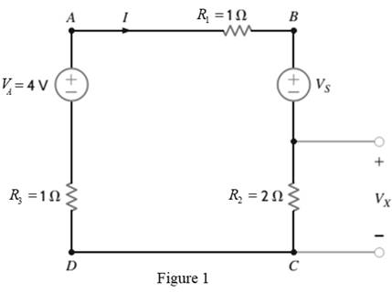
P 4.4-21 Determine the values of the node voltages V1, V2, and
v3 for the circuit shown in Figure P 4.4-21.
29
ww
12 V
+51
Aia
ww
22.
+21
ΖΩ
www
ΖΩ
w
+371
①1
1 A
1. What is the theoretical attenuation of the output voltage at the resonant frequency? Answer to within 1%, or enter 0, or infinity (as “inf”)
Attenuation =
Chapter 2 Solutions
Basic Engineering Circuit Analysis
Ch. 2 - Determine the current and power dissipated in the...Ch. 2 - Determine the voltage across the resistor in Fig....Ch. 2 - In the network in Fig. P2.3, the power absorbed by...Ch. 2 - In the network in Fig. P2.4, the power absorbed by...Ch. 2 - A model for a standard two D-cell flashlight is...Ch. 2 - An automobile uses two halogen headlights...Ch. 2 - Many years ago a string of Christmas tree lights...Ch. 2 - Find I1,I2, and I3 in the network in Fig.P2.8.Ch. 2 - Find I1 in the network in Fig.P2.9.Ch. 2 - Find I1 in the network in Fig.P2.10.
Ch. 2 - Find I1 in the circuit in Fig.P2.11.Ch. 2 - Find I0 and I1 in the circuit in Fig.P2.12.Ch. 2 - Find Ix,Iy, and Iz in the network in Fig.P2.13.Ch. 2 - Find Ix in the circuit in Fig.P2.14.Ch. 2 - Find Ix in the network in Fig. P2.15.Ch. 2 - Find I1 in the network in Fig. P2.16.Ch. 2 - Find Vbd in the circuit in Fig. P2.17.Ch. 2 - Find I1 in the circuit in Fig. P2.18.Ch. 2 - Find I1,I2, and I3 in the network in Fig. P2.19.Ch. 2 - Find Vfb and Vec in the circuit in Fig. P2.20.Ch. 2 - Given the circuit diagram in Fig. P2.21, find the...Ch. 2 - Find VBE and VDA in the circuit in Fig. P2.22.Ch. 2 - Find Vx and Vy in the circuit in Fig. P2.23.Ch. 2 - Find Vac in the circuit in Fig. P2.24.Ch. 2 - Find Vad and Vce in the circuit in Fig. P2.25.Ch. 2 - Find Vo in the circuit in Fig. P2.26.Ch. 2 - Find V1,V2, and V3 in the network in Fig. P2.27.Ch. 2 - Find Vo in the network in Fig. P2.28.Ch. 2 - Find V1,V2, and V3 in the network in Fig. P2.29.Ch. 2 - If Vo=3V in the circuit in Fig. P2.30, find Vs.Ch. 2 - Find the power supplied by each source in the...Ch. 2 - The 10-V source absorbs 2.5-mW of power. Calculate...Ch. 2 - Find Vbd in the network in Fig. P2.33.Ch. 2 - Find V1 in the network in Fig. P2.34.Ch. 2 - Find the power absorbed by the dependent source in...Ch. 2 - In the network in Fig. P2.36, find Vx,VAE, and VBD...Ch. 2 - In the network in Fig. P2.37, find VS if VEB=6V.Ch. 2 - Find VS in the circuit in Fig. P2.38, if VBE=18V.Ch. 2 - Find VA in the network in Fig. P2.39.Ch. 2 - If the 12-V source in the network in Fig. P2.40...Ch. 2 - If VX=12V in the network in Fig. P2.41, find VS...Ch. 2 - Calculate the power absorbed by the dependent...Ch. 2 - Find VA and VO in the circuit in Fig. P2.43.Ch. 2 - Find VO and the power absorbed by the 2k resistor...Ch. 2 - Find the power absorbed or supplied by the 12-V...Ch. 2 - Find Vo in the circuit in Fig. P2.46.Ch. 2 - Find I0 in the network in Fig. P2.47.Ch. 2 - Find Io in the network in Fig. P2.48.Ch. 2 - Find the power supplied by each source in the...Ch. 2 - Find the current IA in the circuit in Fig. P2.50.Ch. 2 - Find IS in the network in Fig. P2.51.Ch. 2 - Find Io in the circuit in Fig. P2.52.Ch. 2 - Find Io in the network in Fig. P2.53.Ch. 2 - Find Vo in the circuit in Fig. P2.54.Ch. 2 - Find Vo in the network in Fig. P2.55.Ch. 2 - Find Io in the network in Fig. P2.56.Ch. 2 - Find Io in the network in Fig. P2.57.Ch. 2 - Find IL in the circuit in Fig. P2.58.Ch. 2 - Find RAB in the network in Fig. P2.59.Ch. 2 - Find RAB in the circuit in Fig. P2.60.Ch. 2 - Find RAB in the circuit in Fig. P2.61.Ch. 2 - Find RAB in the network in Fig. P2.62.Ch. 2 - Find RAB in the circuit in Fig. P2.63.Ch. 2 - Find RAB in the circuit in Fig. P2.64.Ch. 2 - Find RAB in the circuit in Fig. P2.65.Ch. 2 - Find the equivalent resistance Req in the network...Ch. 2 - Find RAB in the network in Fig. P2.67.Ch. 2 - Given the resistor configuration shown in Fig....Ch. 2 - Determine the total resistance, RT, in the circuit...Ch. 2 - Determine the total resistance, RT, in the circuit...Ch. 2 - Determine the total resistance, RT, in the circuit...Ch. 2 - Find the power supplied by the source in the...Ch. 2 - Find I1 and Vo in the circuit in Fig. P2.73.Ch. 2 - Find I1 and Vo in the circuit in Fig. P2.74.Ch. 2 - Find Vab and Vdc in the circuit in Fig. P2.75.Ch. 2 - Find Io in the network in Fig. P2.76.Ch. 2 - Find Io in the circuit in Fig. P2.77.Ch. 2 - Find V1 in the network in Fig. P2.78.Ch. 2 - Find Vab in the circuit in Fig. P2.79.Ch. 2 - Find Vab in the network in Fig. P2.80.Ch. 2 - Find I1,I2, and V1 in the circuit in Fig. P2.81.Ch. 2 - Determine Vo in the network in Fig. P2.82.Ch. 2 - Calculate VAB in Fig. P2.83.Ch. 2 - Find Io in the network in Fig. P2.84 if all...Ch. 2 - Find Io in the circuit in Fig. P2.85.Ch. 2 - Determine the power supplied by the 36-V source in...Ch. 2 - Find the power supplied by the current source in...Ch. 2 - In the network in Fig. P2.88, V1=12V. Find VS.Ch. 2 - In the circuit in Fig. P2.89, Vo=2V. Find IS.Ch. 2 - In the network in Fig. P2.90, V1=14V. Find VS.Ch. 2 - If VR=15V, find VX in Fig. P2.91.Ch. 2 - Find the value of IA in the network in Fig. P2.92.Ch. 2 - If V1=5V in the circuit in Fig. P2.93, find IS.Ch. 2 - Given that Vo=4V in the network in Fig. P2.94,...Ch. 2 - Find the value of VS in the network in Fig. P2.95...Ch. 2 - In the network in Fig. P2.96, VO=6V. Find IS.Ch. 2 - Find the value of V1 in the network in Fig. P2.97...Ch. 2 - Find the value of IA in the circuit in Fig. P2.98.Ch. 2 - If the power supplied by the 2-A current source is...Ch. 2 - The 40-V source in the circuit in Fig. P2.100 is...Ch. 2 - Find the value of the current source IA in the...Ch. 2 - Given Io=2mA in the network in Fig. P2.102, find...Ch. 2 - Find the value of Vx in the network in Fig....Ch. 2 - Given Ia=2mA in the circuit in Fig. P2.104, find...Ch. 2 - Given Va in the network in Fig. 2.105, find IA.Ch. 2 - Find the value of Vx in the circuit in Fig. P2.106...Ch. 2 - Find the power absorbed by the network in Fig....Ch. 2 - Find the value of g in the network in Fig. P2.108...Ch. 2 - Find the power supplied by the 24-V source in the...Ch. 2 - Find Io in circuit in Fig. P2.110.Ch. 2 - Find Io in circuit in Fig. P2.111.Ch. 2 - Determine the value of Vo in the network in Fig....Ch. 2 - If Vo in the circuit in Fig. P2.113 is 24 V, find...Ch. 2 - Find the value of VS in the network in Fig....Ch. 2 - Find the power supplied by the 6-mA source in the...Ch. 2 - Find Vo in the circuit in Fig. P2.116.Ch. 2 - Find Vo in the network in Fig. P2.117.Ch. 2 - Find I1 in the network in Fig. P2.118.Ch. 2 - A single-stage transistor amplifier is modeled as...Ch. 2 - Find Io in the circuit in Fig. P2.120.Ch. 2 - Find Vo in the circuit in Fig. P2.121.Ch. 2 - A typical transistor amplifier is shown in Fig....Ch. 2 - Find VX in the network in Fig. P2.123.Ch. 2 - Find Vo in the network in Fig. P2.124.Ch. 2 - Find I1,I2, and I3 in the circuit in Fig. P2.125.Ch. 2 - Find Io in the network in Fig. P2.126.Ch. 2 - Find the power absorbed by the 12-k resistor on...Ch. 2 - Find the power absorbed by the 12-k resistor in...Ch. 2 - Find the value of k in the network in Fig. P2.129...Ch. 2 - If the power absorbed by the 10-V source in Fig....Ch. 2 - If the power supplied by the 2-A current source in...Ch. 2 - What is the power generated by the source in the...Ch. 2 - Find v ah in the circuit in Fig. 2PFE-2. a. 5V c....Ch. 2 - If Req=10.8 in the circuit in Fig. 2PFE-3, what is...Ch. 2 - Find the equivalent resistance of the circuit in...Ch. 2 - The 100-V source is absorbing 50W of power in the...Ch. 2 - Find the power supplied by the 40-V source in the...Ch. 2 - What is the current I0 in the circuit in Fig....Ch. 2 - Find the voltage Vo in the network in Fig. 2PFE-8....Ch. 2 - What is the voltage Vo in the circuit in Fig....Ch. 2 - Find the current Ix in Fig. 2PFE-10. a. 1/2Ac....
Additional Engineering Textbook Solutions
Find more solutions based on key concepts
In the following exercises, write a program to carry out the task. The program should use variables for each of...
Introduction To Programming Using Visual Basic (11th Edition)
If a class object is dynamically allocated in memory, does its constructor execute? If so, when?
Starting Out with C++ from Control Structures to Objects (9th Edition)
2-1 List the five types of measurements that form the
basis of traditional ptane surveying-
Elementary Surveying: An Introduction To Geomatics (15th Edition)
What is attrition in an abrasive grit?
Degarmo's Materials And Processes In Manufacturing
Write an SQL statement to display the breed, type, and DOB for all pets having the type Dog and the breed Std. ...
Database Concepts (8th Edition)
What do the Ada and COBOL languages have in common?
Concepts Of Programming Languages
Knowledge Booster


Learn more about
Need a deep-dive on the concept behind this application? Look no further. Learn more about this topic, electrical-engineering and related others by exploring similar questions and additional content below.Similar questions
- What is the settling time for your output signal (BRF_OUT)? For this question, We define the settling time as the period of time it has taken for the output to settle into a steady state - ie when your oscillation first decays (aka reduces) to less than approximately 1/20 (5%) of the initial value. (a) Settling time = 22 μs Your last answer was interpreted as follows: Incorrect answer. Check 22 222 What is the peak to peak output voltage (BRF_OUT pp) at the steady state condition? You may need to use the zoom function to perform this calculation. Select a time point that is two times the settling time you answered in the question above. Answer to within 10% accuracy. (a) BRF_OUT pp= mVpp As you may have noticed, the output voltage amplitude is a tiny fraction of the input voltage, i.e. it has been significantly attenuated. Calculate the attenuation (decibels = dB) in the output signal as compared to the input based on the formula given below. Answer to within 1% accuracy.…arrow_forwardmy previous answers for a,b,d were wrong a = 1050 b = 950 d=9.99 c was the only correct value i got previously c = 100hz is correctarrow_forwardV₁(t) ww ZRI ZLI ZL2 ZTH Zci VTH Zc21 Figure 8. Circuit diagram showing calculation approach for VTH and Z TH we want to create a blackbox for the red region, we want to use the same input signal conditions as previously the design of your interference ector circuit: Sine wave with a 1 Vpp, with a frequency of 100 kHz (interference) Square wave with 2.4Vpp, with a frequency of 10 kHz (signal) member an AC Thevenin equivalent is only valid at one frequency. We have chosen to calculate the Thevenin equivalent circuit (and therefore the ackbox) at the interference frequency (i.e. 100 kHz), and the signal frequency (i.e. 10 kHz) as these are the key frequencies to analyse. Your boss is assured you that the waveform converter module has been pre-optimised to the DAB Receiver if you use the recommended circuit topology.arrow_forward
- Vs(t) + v(t) + vi(t) ZR ZL Figure 1: Second order RLC circuit Zc + ve(t) You are requested to design the circuit shown in Figure 1. The circuit is assumed to be operating at its resonant frequency when it is fed by a sinusoidal voltage source Vs (t) = 2sin(le6t). To help design your circuit you have been given the value of inductive reactance ZL = j1000. Assume that the amplitude of the current at resonance is Is (t) = 2 mA. Based on this information, answer the following to help design your circuit. Use cartesian notation for your answers, where required.arrow_forwardWhat is the attenuation at the resonant frequency? You should use the LTSpice cursors for your measurement. Answer to within 1% accuracy, or enter 0, or infinity (as "inf") (a) Attenuation (dB) = dB Check You may have noticed that it was significantly easier to use frequency-domain "AC" simulation to measure the attenuation, compared to the steps we performed in the last few questions. (i.e. via a time-domain "transient" simulation). AC analysis allows us to observe and quantify large scale positive or negative changes in a signal of interest across a wide range of different frequencies. From the response you will notice that only frequencies that are relatively close to 100 kHz have been attenuated. This is the result of the Band-reject filter you have designed, and shows the 'rejection' (aka attenuation) of any frequencies that lie in a given band. The obvious follow-up question is how do we define this band? We use a quantity known as the bandwidth. A commonly used measurement for…arrow_forwardV₁(t) ww ZRI ZLI ZL2 ZTH Zci VTH Zc21 Figure 8. Circuit diagram showing calculation approach for VTH and Z TH we want to create a blackbox for the red region, we want to use the same input signal conditions as previously the design of your interference ector circuit: Sine wave with a 1 Vpp, with a frequency of 100 kHz (interference) Square wave with 2.4Vpp, with a frequency of 10 kHz (signal) member an AC Thevenin equivalent is only valid at one frequency. We have chosen to calculate the Thevenin equivalent circuit (and therefore the ackbox) at the interference frequency (i.e. 100 kHz), and the signal frequency (i.e. 10 kHz) as these are the key frequencies to analyse. Your boss is assured you that the waveform converter module has been pre-optimised to the DAB Receiver if you use the recommended circuit topology.arrow_forward
- Vs(t) + v(t) + vi(t) ZR ZL Figure 1: Second order RLC circuit Zc + ve(t) You are requested to design the circuit shown in Figure 1. The circuit is assumed to be operating at its resonant frequency when it is fed by a sinusoidal voltage source Vs (t) = 2sin(le6t). To help design your circuit you have been given the value of inductive reactance ZL = j1000. Assume that the amplitude of the current at resonance is Is (t) = 2 mA. Based on this information, answer the following to help design your circuit. Use cartesian notation for your answers, where required.arrow_forwardFor a band-rejection filter, the response drops below this half power point at two locations as visualised in Figure 7, we need to find these frequencies. Let's call the lower frequency-3dB point as fr and the higher frequency -3dB point fH. We can then find out the bandwidth as f=fHfL, as illustrated in Figure 7. 0dB Af -3 dB Figure 7. Band reject filter response diagram Considering your AC simulation frequency response and referring to Figure 7, measure the following from your AC simulation. 1% accuracy: (a) Upper-3db Frequency (fH) = Hz (b) Lower-3db Frequency (fL) = Hz (c) Bandwidth (Aƒ) = Hz (d) Quality Factor (Q) =arrow_forwardV₁(t) ww ZRI ZLI Z12 Zci Zcz Figure 4. Notch filter circuit topology ши Consider the second order resonant circuit shown in Figure 4. Impedances ZLIZ C1. ZL2. Z c2 combine together forming a two-stage "band- reject" filter, so called because it rejects a "band" (aka range) of frequencies. This circuit topology is also commonly referred to as a "band-stop" filter or "notch" filter. The output of the DAB receiver block has been approximated via Thevenin's theorem for you as a voltage source Vs (t) and associated series impedance Z RI To succeed in our goal, we are going to use an iterative design approach. First we will design the interference rejector, and then repeat the process, using the output of the interference rejector to check the provided waveform converter works as intended.arrow_forward
- 1. What is the settling time for your output signal (BRF_OUT)? For this question, We define the settling time as the period of time it has taken for the output to settle into a steady state - ie when your oscillation first decays (aka reduces) to less than approximately 1/20 (5%) of the initial value. (a) Settling timearrow_forward2. What is the total impedance Zt of your designed circuit? Represent your result in cartesian form NOTE: use j to represent sqare root Zt=arrow_forwardAn electric resistance space heater is designed such that it resembles a rectangular box 55 cm high, 75 cm long, and 20 cm wide filled with 45 kg of oil. The heater is to be placed against a wall, and thus heat transfer from its back surface is negligible. The surface temperature of the heater is not to exceed 75°C in a room at 25°C for safety considerations. The emissivity of the outer surface of the heater is 0.8 and the average temperature of the ceiling and wall surfaces is the same as the room air temperature. The properties of air at 1 atm and the film temperature are: k = 0.02753 W/m-°C, v=1.798 x 10⁻⁵ m²/s, Pr = 0.7228, and ẞ= 0.003096K-1 Wall T₁ =75°C Oil € = 0.8 Electric heater Heating element Disregarding heat transfer from the bottom and top surfaces of the heater in anticipation that the top surface will be used as a shelf, determine the power rating of the heater in W. The power rating of the heater is W.arrow_forward
arrow_back_ios
SEE MORE QUESTIONS
arrow_forward_ios
Recommended textbooks for you
 Introductory Circuit Analysis (13th Edition)Electrical EngineeringISBN:9780133923605Author:Robert L. BoylestadPublisher:PEARSON
 Delmar's Standard Textbook Of ElectricityElectrical EngineeringISBN:9781337900348Author:Stephen L. HermanPublisher:Cengage Learning
 Programmable Logic ControllersElectrical EngineeringISBN:9780073373843Author:Frank D. PetruzellaPublisher:McGraw-Hill Education
 Fundamentals of Electric CircuitsElectrical EngineeringISBN:9780078028229Author:Charles K Alexander, Matthew SadikuPublisher:McGraw-Hill Education
 Electric Circuits. (11th Edition)Electrical EngineeringISBN:9780134746968Author:James W. Nilsson, Susan RiedelPublisher:PEARSON
 Engineering ElectromagneticsElectrical EngineeringISBN:9780078028151Author:Hayt, William H. (william Hart), Jr, BUCK, John A.Publisher:Mcgraw-hill Education,
Introductory Circuit Analysis (13th Edition)
Electrical Engineering
ISBN:9780133923605
Author:Robert L. Boylestad
Publisher:PEARSON
Delmar's Standard Textbook Of Electricity
Electrical Engineering
ISBN:9781337900348
Author:Stephen L. Herman
Publisher:Cengage Learning
Programmable Logic Controllers
Electrical Engineering
ISBN:9780073373843
Author:Frank D. Petruzella
Publisher:McGraw-Hill Education
Fundamentals of Electric Circuits
Electrical Engineering
ISBN:9780078028229
Author:Charles K Alexander, Matthew Sadiku
Publisher:McGraw-Hill Education
Electric Circuits. (11th Edition)
Electrical Engineering
ISBN:9780134746968
Author:James W. Nilsson, Susan Riedel
Publisher:PEARSON
Engineering Electromagnetics
Electrical Engineering
ISBN:9780078028151
Author:Hayt, William H. (william Hart), Jr, BUCK, John A.
Publisher:Mcgraw-hill Education,
Lesson 2 - Source Transformations, Part 2 (Engineering Circuits); Author: Math and Science;https://www.youtube.com/watch?v=7gno74RhVGQ;License: Standard Youtube License